- 您現(xiàn)在的位置:買賣IC網(wǎng) > PDF目錄384756 > MT49H32M9CFM-xx (Micron Technology, Inc.) 288Mb SIO REDUCED LATENCY(RLDRAM II) PDF資料下載
參數(shù)資料
| 型號: | MT49H32M9CFM-xx |
| 廠商: | Micron Technology, Inc. |
| 英文描述: | 288Mb SIO REDUCED LATENCY(RLDRAM II) |
| 中文描述: | 288Mb二氧化硅約化延遲(延遲DRAM二) |
| 文件頁數(shù): | 21/44頁 |
| 文件大?。?/td> | 1117K |
| 代理商: | MT49H32M9CFM-XX |
第1頁第2頁第3頁第4頁第5頁第6頁第7頁第8頁第9頁第10頁第11頁第12頁第13頁第14頁第15頁第16頁第17頁第18頁第19頁第20頁當(dāng)前第21頁第22頁第23頁第24頁第25頁第26頁第27頁第28頁第29頁第30頁第31頁第32頁第33頁第34頁第35頁第36頁第37頁第38頁第39頁第40頁第41頁第42頁第43頁第44頁
16 MEG x 18, 32 MEG x 9
2.5V V
EXT
, 1.8V V
DD
, HSTL, SIO, RLDRAM II
pdf: 09005aef80a41b59/zip: 09005aef811ba111
MT49H8M18C_2.fm - Rev. F 11/04 EN
Micron Technology, Inc., reserves the right to change products or specifications without notice.
2004 Micron Technology, Inc. All rights reserved.
21
Read Basic Information
Read accesses are initiated with a READ command,
as shown in Figure 17. Row and bank addresses are
provided with the READ command.
During READ bursts, the memory device drives the
read data edge-aligned with the QK signal. After a pro-
grammable read latency, data is available at the out-
puts. The data valid signal indicates that valid data will
be present in the next half clock cycle.
The skew between QK and the crossing point of CK
is specified as
t
CKQK.
t
QKQ0 is the skew between QK0
and the last valid data edge considered over all the
data generated at the Q signals.
t
QKQ1 is the skew
between QK1 and the last valid data edge considered
over all the data generated at the Q signals.
t
QKQx is
derived at each QKx clock edge and is not cumulative
over time.
t
QKQ is the maximum of
t
QKQ0 and
t
QKQ1.
After completion of a burst, assuming no other
commands have been initiated, output data (Q) will go
High-Z. Back-to-back READ commands are possible,
producing a continuous flow of output data.
The data valid window is derived from each QK
transition and is defined as:
MIN (
t
QKH,
t
QKL) - 2(
t
QKQ [MAX]).
Any READ burst may be followed by a subsequent
WRITE command. Figures 21 and 22 illustrate the tim-
ing requirements for a READ followed by a WRITE.
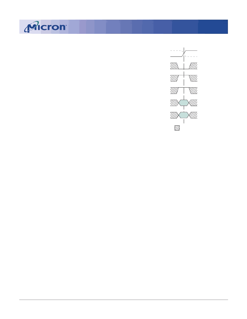
Figure 17: READ Command
NOTE:
A: address; BA: bank address.
CK#
CK
WE#
REF#
CS#
A
BA
A(20:0)
BA(2:0)
DON’T CARE
相關(guān)PDF資料 |
PDF描述 |
|---|---|
| MT4C1004J | 4 Meg x 1 FPM DRAM(4 M x 1快速頁面模式動(dòng)態(tài)RAM) |
| MT4C4001STG-6 | standard or self refresh |
| MT4C4001STG-7 | standard or self refresh |
| MT4C4001STG-8 | standard or self refresh |
| MT4C4001JDJ-6 | standard or self refresh |
相關(guān)代理商/技術(shù)參數(shù) |
參數(shù)描述 |
|---|---|
| MT49H32M9CHU-25 | 制造商:Micron Technology Inc 功能描述:DRAM CHIP RLDRAM 288MBIT 1.8V 144FBGA - Trays |
| MT49H32M9CHU-33 | 制造商:Micron Technology Inc 功能描述:32MX9 RLDRAM PLASTIC FBGA 1.8V SEPARATE I/O 8 BANKS 1.8V I/O - Trays |
| MT49H32M9CHU-5 | 制造商:Micron Technology Inc 功能描述:32MX9 RLDRAM PLASTIC FBGA 1.8V SEPARATE I/O 8 BANKS 1.8V I/O - Trays |
| MT49H32M9FM-25 | 制造商:Micron Technology Inc 功能描述: |
| MT49H32M9FM-25 TR | 功能描述:IC RLDRAM 288MBIT 400MHZ 144FBGA RoHS:是 類別:集成電路 (IC) >> 存儲(chǔ)器 系列:- 產(chǎn)品變化通告:Product Discontinuation 05/Nov/2008 標(biāo)準(zhǔn)包裝:84 系列:- 格式 - 存儲(chǔ)器:RAM 存儲(chǔ)器類型:SRAM - 同步 ZBT 存儲(chǔ)容量:4.5M(128K x 36) 速度:75ns 接口:并聯(lián) 電源電壓:3.135 V ~ 3.465 V 工作溫度:-40°C ~ 85°C 封裝/外殼:119-BGA 供應(yīng)商設(shè)備封裝:119-PBGA(14x22) 包裝:托盤 其它名稱:71V3557SA75BGI |
發(fā)布緊急采購,3分鐘左右您將得到回復(fù)。