- 您現(xiàn)在的位置:買賣IC網(wǎng) > PDF目錄384756 > MT49H32M9CFM-xx (Micron Technology, Inc.) 288Mb SIO REDUCED LATENCY(RLDRAM II) PDF資料下載
參數(shù)資料
| 型號: | MT49H32M9CFM-xx |
| 廠商: | Micron Technology, Inc. |
| 英文描述: | 288Mb SIO REDUCED LATENCY(RLDRAM II) |
| 中文描述: | 288Mb二氧化硅約化延遲(延遲DRAM二) |
| 文件頁數(shù): | 13/44頁 |
| 文件大小: | 1117K |
| 代理商: | MT49H32M9CFM-XX |
第1頁第2頁第3頁第4頁第5頁第6頁第7頁第8頁第9頁第10頁第11頁第12頁當(dāng)前第13頁第14頁第15頁第16頁第17頁第18頁第19頁第20頁第21頁第22頁第23頁第24頁第25頁第26頁第27頁第28頁第29頁第30頁第31頁第32頁第33頁第34頁第35頁第36頁第37頁第38頁第39頁第40頁第41頁第42頁第43頁第44頁
16 MEG x 18, 32 MEG x 9
2.5V V
EXT
, 1.8V V
DD
, HSTL, SIO, RLDRAM II
pdf: 09005aef80a41b59/zip: 09005aef811ba111
MT49H8M18C_2.fm - Rev. F 11/04 EN
Micron Technology, Inc., reserves the right to change products or specifications without notice.
2004 Micron Technology, Inc. All rights reserved.
13
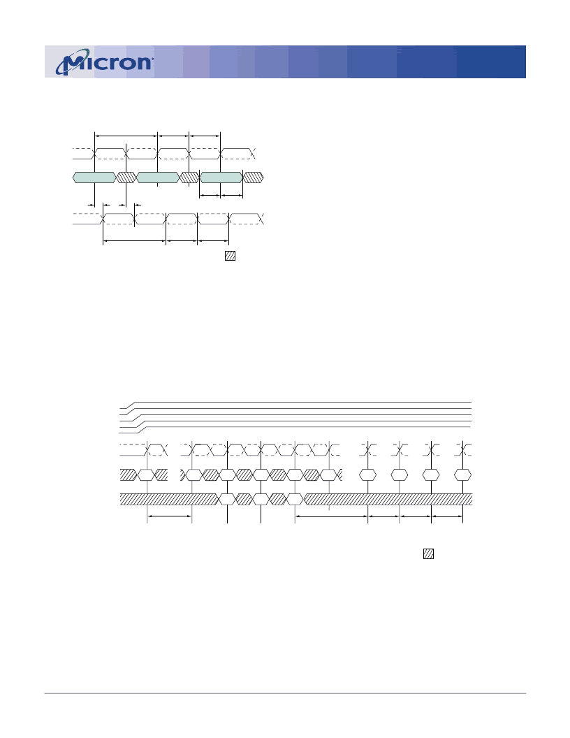
Figure 5: Clock/Input Data Clock
Command/Address Timings
Initialization
The RLDRAM must be powered up and initialized in
a predefined manner. Operational procedures other
than those specified may result in undefined opera-
tions or permanent damage to the device.
The following sequence is used for power-up:
1. Apply power (V
EXT
, V
DD
, V
DD
Q, V
REF
, V
TT
) and
start clock as soon as the supply voltages are sta-
ble. Apply V
DD
and V
EXT
before or at the same
time as V
DD
Q. Apply V
DD
Q before or at the same
time as V
REF
and V
TT
. Although there is no timing
relation between V
EXT
and V
DD
, the chip starts
the power-up sequence only after both voltages
are at their nominal levels. The pad supply must
not be applied before the core supplies. Maintain
all remaining balls in NOP conditions.
2. Maintain stable conditions for 200μs (MIN).
3. Issue three MRS commands: two dummies plus
one valid MRS.
4.
t
MRSC after the valid MRS, issue eight Auto
Refresh commands, one on each bank and sepa-
rated by 2,048 cycles. Initial bank refresh order
does not matter.
5. After
t
RC, the chip is ready for normal operation.
Figure 6: Power-Up Sequence
CK#
CK
t
CKH
t
CKL
t
AH
t
AS
t
CK
CMD,
ADDR
DKx#
DKx
t
CKDK
t
CKDK
DON’T CARE
t
DKH
t
DKL
t
DK
VALID
VALID
VALID
V
EXT
V
DD
V
DD
Q
V
REF
V
TT
CK#
CK
CMD
200μs MIN
t
MRSC
t
RC
2,048
cycles
MIN
6 × 2,048
cycles
MIN
MRS
MRS
MRS
RF0
RF1
RF7
AC
DON’T CARE
ADD
NOP
NOP
NOP
MRS: MRS command
RFx: REFRESH Bank x
AC: Any command
相關(guān)PDF資料 |
PDF描述 |
|---|---|
| MT4C1004J | 4 Meg x 1 FPM DRAM(4 M x 1快速頁面模式動態(tài)RAM) |
| MT4C4001STG-6 | standard or self refresh |
| MT4C4001STG-7 | standard or self refresh |
| MT4C4001STG-8 | standard or self refresh |
| MT4C4001JDJ-6 | standard or self refresh |
相關(guān)代理商/技術(shù)參數(shù) |
參數(shù)描述 |
|---|---|
| MT49H32M9CHU-25 | 制造商:Micron Technology Inc 功能描述:DRAM CHIP RLDRAM 288MBIT 1.8V 144FBGA - Trays |
| MT49H32M9CHU-33 | 制造商:Micron Technology Inc 功能描述:32MX9 RLDRAM PLASTIC FBGA 1.8V SEPARATE I/O 8 BANKS 1.8V I/O - Trays |
| MT49H32M9CHU-5 | 制造商:Micron Technology Inc 功能描述:32MX9 RLDRAM PLASTIC FBGA 1.8V SEPARATE I/O 8 BANKS 1.8V I/O - Trays |
| MT49H32M9FM-25 | 制造商:Micron Technology Inc 功能描述: |
| MT49H32M9FM-25 TR | 功能描述:IC RLDRAM 288MBIT 400MHZ 144FBGA RoHS:是 類別:集成電路 (IC) >> 存儲器 系列:- 產(chǎn)品變化通告:Product Discontinuation 05/Nov/2008 標(biāo)準(zhǔn)包裝:84 系列:- 格式 - 存儲器:RAM 存儲器類型:SRAM - 同步 ZBT 存儲容量:4.5M(128K x 36) 速度:75ns 接口:并聯(lián) 電源電壓:3.135 V ~ 3.465 V 工作溫度:-40°C ~ 85°C 封裝/外殼:119-BGA 供應(yīng)商設(shè)備封裝:119-PBGA(14x22) 包裝:托盤 其它名稱:71V3557SA75BGI |
發(fā)布緊急采購,3分鐘左右您將得到回復(fù)。