- 您現(xiàn)在的位置:買賣IC網(wǎng) > PDF目錄1956 > MSC8103VT1200F (Freescale Semiconductor)IC DSP 16BIT 300MHZ 332-FCPBGA PDF資料下載
參數(shù)資料
| 型號: | MSC8103VT1200F |
| 廠商: | Freescale Semiconductor |
| 文件頁數(shù): | 4/104頁 |
| 文件大?。?/td> | 0K |
| 描述: | IC DSP 16BIT 300MHZ 332-FCPBGA |
| 標準包裝: | 90 |
| 系列: | StarCore |
| 類型: | SC140 內(nèi)核 |
| 接口: | 通信處理器模塊(CPM) |
| 時鐘速率: | 300MHz |
| 非易失內(nèi)存: | 外部 |
| 芯片上RAM: | 512kB |
| 電壓 - 輸入/輸出: | 3.30V |
| 電壓 - 核心: | 1.60V |
| 工作溫度: | -40°C ~ 75°C |
| 安裝類型: | 表面貼裝 |
| 封裝/外殼: | 332-BFBGA,F(xiàn)CPBGA |
| 供應(yīng)商設(shè)備封裝: | 332-FCBGA(17x17) |
| 包裝: | 托盤 |
第1頁第2頁第3頁當前第4頁第5頁第6頁第7頁第8頁第9頁第10頁第11頁第12頁第13頁第14頁第15頁第16頁第17頁第18頁第19頁第20頁第21頁第22頁第23頁第24頁第25頁第26頁第27頁第28頁第29頁第30頁第31頁第32頁第33頁第34頁第35頁第36頁第37頁第38頁第39頁第40頁第41頁第42頁第43頁第44頁第45頁第46頁第47頁第48頁第49頁第50頁第51頁第52頁第53頁第54頁第55頁第56頁第57頁第58頁第59頁第60頁第61頁第62頁第63頁第64頁第65頁第66頁第67頁第68頁第69頁第70頁第71頁第72頁第73頁第74頁第75頁第76頁第77頁第78頁第79頁第80頁第81頁第82頁第83頁第84頁第85頁第86頁第87頁第88頁第89頁第90頁第91頁第92頁第93頁第94頁第95頁第96頁第97頁第98頁第99頁第100頁第101頁第102頁第103頁第104頁
Layout Practices
MSC8103 Network Digital Signal Processor, Rev. 12
Freescale Semiconductor
4-3
Since the address pins switch once at every second cycle, the address pins frequency is a quarter of the bus
frequency (that is, 25 MHz).
For the same reason the data pins frequency is 3.125 MHz.
Calculating internal power (from Table 2-5 values):
PCORE (200) = ((PCORE – PLCO)/300) × 200 + PLCO =((450 – 3) / 300 × 200 + 3 = 301
PCPM (100) = ((PCPM – PLCP) / 200) × 100 + PLCP = ((320 – 6) / 200) × 100 + 6 = 163
PSIU (50) = ((PSIU – PLSI) / 100) × 50 + PLSI = ((80 – 2) / 100) × 50 + 2 = 41
PINT = PCORE(200) + PCPM(100) + PSIU(50) = 301 + 163 + 41 = 505
PD = PINT + PI/O = 505 + 67 = 572
Maximum allowed ambient temperature is:
TA = TJ – (PD × θJA)
4.4 Layout Practices
Each VCC and VDD pin on the MSC8103 should be provided with a low-impedance path to the board’s power
supply. Similarly, each GND pin should be provided with a low-impedance path to ground. The power supply pins
drive distinct groups of logic on the chip. The VCC power supply should be bypassed to ground using at least four
0.1 F by-pass capacitors located as closely as possible to the four sides of the package. The capacitor leads and
associated printed circuit traces connecting to chip VCC, VDD, and GND should be kept to less than half an inch per
capacitor lead. A four-layer board is recommended, employing two inner layers as VCC and GND planes.
All output pins on the MSC8103 have fast rise and fall times. Printed circuit board (PCB) trace interconnection
length should be minimized in order to minimize undershoot and reflections caused by these fast output switching
times. This recommendation particularly applies to the address and data busses. Maximum PCB trace lengths of six
inches are recommended. Capacitance calculations should consider all device loads as well as parasitic
capacitances due to the PCB traces. Attention to proper PCB layout and bypassing becomes especially critical in
systems with higher capacitive loads because these loads create higher transient currents in the VCC, VDD, and GND
circuits. Pull up all unused inputs or signals that will be inputs during reset. Special care should be taken to
minimize the noise levels on the PLL supply pins.
There are 2 pairs of PLL supply pins: VCCSYN-GNDSYN and VCCSYN1-GNDSYN1. Each pair supplies one PLL. To
ensure internal clock stability, filter the power to the VCCSYN and VCCSYN1 inputs with a circuit similar to the one in
Figure 4-2. To filter as much noise as possible, place the circuit as close as possible to VCCSYN and VCCSYN1. The
0.01-F capacitor should be closest to VCCSYN and VCCSYN1, followed by the 10-F capacitor, the 10-nH inductor,
and finally the 10-
Ω resistor to V
DD. These traces should be kept short and direct.
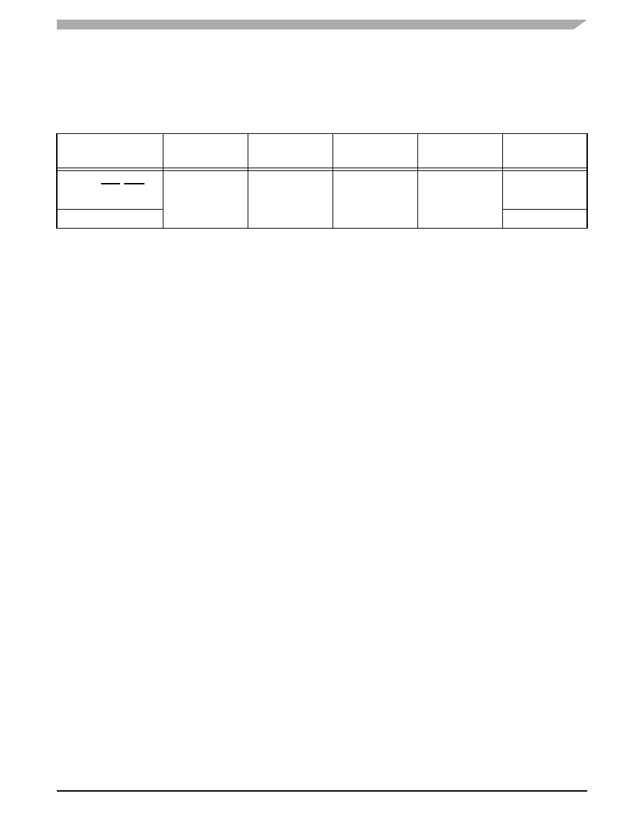
Table 4-1.
Power Dissipation
Pins
Number of Pins
Switching
× C
× VDDH2
× f × 10–3
Power in mW
Address
Data, HRD, HRW
CLKOUT
4
34
1
× 30
× 3.32
× 12.5 × 10–3
× 3. 125 × 10–3
× 50 × 10–3
16.25
34.75
16
Total PI/O
67
相關(guān)PDF資料 |
PDF描述 |
|---|---|
| MSC8112TVT2400V | DSP DUAL CORE 431-FCPBGA |
| MSC8113TVT4800V | DSP TRI-CORE 431-FCPBGA |
| MSC8122MP8000 | DSP 16BIT 500MHZ MULTI 431FCPBGA |
| MSC8144VT800A | IC DSP QUAD 800MHZ 783FCBGA |
| MSC8154SVT1000B | IC PROCESSOR QUAD DGTL 783FCPBGA |
相關(guān)代理商/技術(shù)參數(shù) |
參數(shù)描述 |
|---|---|
| MSC81058 | 制造商:STMICROELECTRONICS 制造商全稱:STMicroelectronics 功能描述:RF & MICROWAVE TRANSISTORS GENERAL PURPOSE AMPLIFIER APPLICATIONS |
| MSC81090 | 制造商:ASI 制造商全稱:ASI 功能描述:NPN SILICON RF POWER TRANSISTOR |
| MSC81111 | 制造商:STMICROELECTRONICS 制造商全稱:STMicroelectronics 功能描述:RF & MICROWAVE TRANSISTORS GENERAL PURPOSE AMPLIFIER APPLICATIONS |
| MSC81118 | 制造商:STMICROELECTRONICS 制造商全稱:STMicroelectronics 功能描述:RF & MICROWAVE TRANSISTORS GENERAL PURPOSE AMPLIFIER APPLICATIONS |
| MSC8112 | 制造商:FREESCALE 制造商全稱:Freescale Semiconductor, Inc 功能描述:Dual Core Digital Signal Processor |
發(fā)布緊急采購,3分鐘左右您將得到回復(fù)。