- 您現(xiàn)在的位置:買賣IC網(wǎng) > PDF目錄296460 > MAX1359ACTL+ (MAXIM INTEGRATED PRODUCTS INC) SPECIALTY ANALOG CIRCUIT, QCC40 PDF資料下載
參數(shù)資料
| 型號: | MAX1359ACTL+ |
| 廠商: | MAXIM INTEGRATED PRODUCTS INC |
| 元件分類: | 模擬信號調(diào)理 |
| 英文描述: | SPECIALTY ANALOG CIRCUIT, QCC40 |
| 封裝: | 6 X 6 MM, 0.80 MM HEIGHT, MO220, TQFN-40 |
| 文件頁數(shù): | 52/74頁 |
| 文件大小: | 1214K |
| 代理商: | MAX1359ACTL+ |
第1頁第2頁第3頁第4頁第5頁第6頁第7頁第8頁第9頁第10頁第11頁第12頁第13頁第14頁第15頁第16頁第17頁第18頁第19頁第20頁第21頁第22頁第23頁第24頁第25頁第26頁第27頁第28頁第29頁第30頁第31頁第32頁第33頁第34頁第35頁第36頁第37頁第38頁第39頁第40頁第41頁第42頁第43頁第44頁第45頁第46頁第47頁第48頁第49頁第50頁第51頁當前第52頁第53頁第54頁第55頁第56頁第57頁第58頁第59頁第60頁第61頁第62頁第63頁第64頁第65頁第66頁第67頁第68頁第69頁第70頁第71頁第72頁第73頁第74頁
MAX1358/MAX1359/MAX1360
16-Bit Data-Acquisition Systems with ADC, DACs,
UPIOs, RTC, Voltage Monitors, and Temp Sensor
56
______________________________________________________________________________________
The switch-control register controls the two SPDT
switches (SPDT1 and SPDT2) and the two DACA and
DACB output buffer SPST switches (SWA and SWB).
Control these switches by the serial bits in this register,
by any of the UPIO pins that are enabled for that func-
tion, or by the PWM.
SWA: (MAX1358/MAX1359) DACA output buffer SPST-
switch A control bit. The SWA bit, the UPIO inputs (if
configured), and the PWM (if configured) control the
state of the SWA switch as shown in Table 17. The
UPIO_ states of 0 and 1 in the table below correspond
to respective deasserted and asserted logic states as
defined by the ALH_ bit of the UPIO_CTRL register. If a
UPIO is not configured for this mode, its value applied
to the table below is 0. The PWM states of 0 and 1 in the
table below correspond to the respective PWM off (or
low) and on (or high) states defined by the SWAH and
SWAL bits (see the PWM_CTRL Register section). If the
PWM is not configured for this mode, its value applied
to the table below is 0. The power-on default is 0.
SWB: (MAX1358 only) DACB output buffer SPST-switch
B control bit. The SWB bit, the UPIO inputs (if config-
ured), and the PWM (if configured) control the state of
the SWB switch as shown in Table 18. The UPIO_ states
of 0 and 1 in the table correspond to respective
deasserted and asserted logic states as defined by the
ALH_ bit (see the UPIO_CTRL Register section). If a
UPIO is not configured for this mode, its value applied
to the table is 0. The PWM states of 0 and 1 in the table
correspond to the respective PWM off (or low) and on
(or high) states defined by the SWBH and SWBL bits
(see the PWM_CTRL Register section). If the PWM is
not configured for this mode, its value applied to the
table is 0. The power-on default is 0.
SPDT1<1:0>: Single-pole double-throw switch 1 con-
trol bits. The SPDT1<1:0> bits, the UPIO pins (if config-
ured), and the PWM (if configured) control the state of
the switch as shown in Table 19. The UPIO_ states of 0
and 1 in the table below correspond to respective
deasserted and asserted logic states as defined by the
ALH_ bit of the UPIO_CTRL register. If a UPIO is not
configured for this mode, its value applied to Table 19
is 0. The PWM states of 0 and 1 in Table 19 below cor-
respond to the respective PWM off (low) and on (high)
states defined by the SPD1 bit in the PWM_CTRL regis-
ter. If the PWM is not configured for this mode, its value
applied to Table 19 is 0. The power-on default is 00.
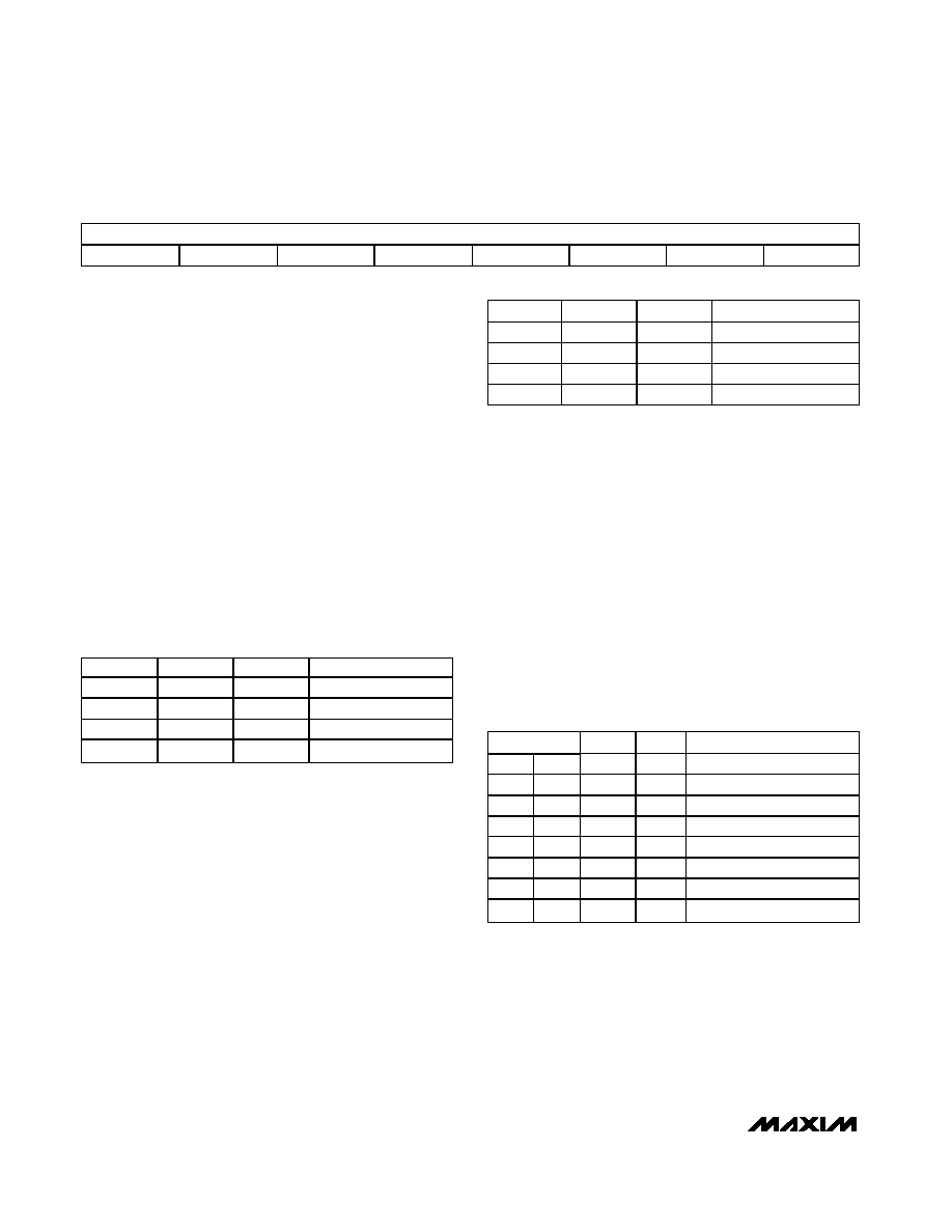
MSB
LSB
SWA
SWB
SPDT11
SPDT10
SPDT21
SPDT20
X
SW_CTRL Register (Power-On State: 0000 00XX)
SWA BIT*
UPIO_*
PWM*
SWA SWITCH STATE
000
Switch open
XX
1
Switch closed
X1
X
Switch closed
1X
X
Switch closed
Table 17. SWA States
X = Don’t care.
*Switch SWA control is effectively an OR of the SWA bit, UPIO
pins, and PWM.
SWB BIT*
UPIO_*
PWM*
SWB SWITCH STATE
00
0
Switch open
XX1
Switch closed
X1
X
Switch closed
1X
X
Switch closed
Table 18. SWB States (MAX1358 Only)
X = Don’t care.
*Switch SWB control is effectively an OR of the SWB bit, UPIO
pins, and PWM.
SPDT1<1:0>
UPIO_*
PWM*
SPDT1 SWITCH STATE
00
SNO1 open, SNC1 open
0X
X
1
SNO1 closed, SNC1 closed
0X
1
X
SNO1 closed, SNC1 closed
01
X
SNO1 closed, SNC1 closed
10
00
SNC1 closed, SNO1 open
1X
X1
SNC1 open, SNO1 closed
1X
SNC1 open, SNO1 closed
11
XX
SNC1 open, SNO1 closed
Table 19. SPDT Switch 1 States
X = Don’t care.
*Switch SPDT1 control is effectively an OR of the SPDT10 bit, the
UPIO pins, and the PWM output. The SPDT11 bit determines if
the switches open and close together or if they toggle.
相關PDF資料 |
PDF描述 |
|---|---|
| MAX16005AUE+ | 6-CHANNEL POWER SUPPLY MANAGEMENT CKT, PDSO16 |
| MAX16005DUE+ | 6-CHANNEL POWER SUPPLY MANAGEMENT CKT, PDSO16 |
| MAX16072RS30D3+ | POWER SUPPLY SUPPORT CKT, PBGA4 |
| MAX17004AETJ+ | 3.3 A DUAL SWITCHING CONTROLLER, 575 kHz SWITCHING FREQ-MAX, QCC32 |
| MAX177ENG | CMOS 10-Bit A/D Converter with Track-and-Hold |
相關代理商/技術參數(shù) |
參數(shù)描述 |
|---|---|
| MAX1359ACTL+ | 制造商:Maxim Integrated Products 功能描述:DATA ACQ SYS SGL ADC SGL DAC 16BIT 40TQFN EP - Rail/Tube |
| MAX1359ACTL+T | 制造商:Maxim Integrated Products 功能描述:DATA ACQ SYS SGL ADC SGL DAC 16BIT 40TQFN EP - Tape and Reel |
| MAX1359ACTL-T | 制造商:Maxim Integrated Products 功能描述:16-BIT DATA-ACQUISITION SYSTEM W ADC,DACS,UPI - Tape and Reel |
| MAX1359AEGL | 制造商:Maxim Integrated Products 功能描述:- Rail/Tube |
| MAX1359AETL | 制造商:Maxim Integrated Products 功能描述:16-BIT DATA-ACQUISITION SYSTEM W ADC,DACS,UPI - Rail/Tube |
發(fā)布緊急采購,3分鐘左右您將得到回復。