- 您現(xiàn)在的位置:買賣IC網(wǎng) > PDF目錄296460 > MAX1359ACTL+ (MAXIM INTEGRATED PRODUCTS INC) SPECIALTY ANALOG CIRCUIT, QCC40 PDF資料下載
參數(shù)資料
| 型號: | MAX1359ACTL+ |
| 廠商: | MAXIM INTEGRATED PRODUCTS INC |
| 元件分類: | 模擬信號調(diào)理 |
| 英文描述: | SPECIALTY ANALOG CIRCUIT, QCC40 |
| 封裝: | 6 X 6 MM, 0.80 MM HEIGHT, MO220, TQFN-40 |
| 文件頁數(shù): | 48/74頁 |
| 文件大?。?/td> | 1214K |
| 代理商: | MAX1359ACTL+ |
第1頁第2頁第3頁第4頁第5頁第6頁第7頁第8頁第9頁第10頁第11頁第12頁第13頁第14頁第15頁第16頁第17頁第18頁第19頁第20頁第21頁第22頁第23頁第24頁第25頁第26頁第27頁第28頁第29頁第30頁第31頁第32頁第33頁第34頁第35頁第36頁第37頁第38頁第39頁第40頁第41頁第42頁第43頁第44頁第45頁第46頁第47頁當前第48頁第49頁第50頁第51頁第52頁第53頁第54頁第55頁第56頁第57頁第58頁第59頁第60頁第61頁第62頁第63頁第64頁第65頁第66頁第67頁第68頁第69頁第70頁第71頁第72頁第73頁第74頁
MAX1358/MAX1359/MAX1360
16-Bit Data-Acquisition Systems with ADC, DACs,
UPIOs, RTC, Voltage Monitors, and Temp Sensor
52
______________________________________________________________________________________
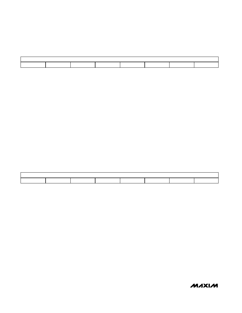
MSB
LSB
UP4MD3
UP4MD2
UP4MD1
UP4MD0
PUP4
SV4
ALH4
LL4
UPIO4_CTRL Register (Power-On State: 0000 1000)
UPIO4_CTRL register. This register configures the
UPIO4 pin functionality.
UP4MD<3:0>: UPIO4-mode selection bits. These bits
configure the mode for the UPIO4 pin. See Table 16 for
a detailed description. The power-on default is 0 hex.
PUP4: Pullup UPIO4 control bit. Set PUP4 = 1 to enable
a weak pullup resistor on the UPIO4 pin and set PUP4 =
0 to disable it. The pullup resistor is connected to either
DVDD or CPOUT as programmed by the SV4 bit. The
pullup is enabled only when UPIO4 is configured as an
input. Open-drain behavior can be simulated at UPIO4
by setting the mode to GPO with LL4 = 0 and by chang-
ing the mode to GPI with PUP4 = 0, allowing external
high pullup. The power-on default is 1.
SV4: Supply-voltage UPIO4 selection bit. Set SV4 = 0
to select DVDD as the supply voltage for the UPIO4 pin
and set SV4 = 1 to select CPOUT as the supply volt-
age. The selected supply voltage applies to all modes
for the UPIO4 pin. The power-on default is 0.
ALH4: Active logic-level assertion high UPIO4 bit. Set
ALH4 = 0 to define the input or output assertion level
for UPIO4 as low except when in GPI and GPO modes.
Set ALH4 = 1 to define the input or output assertion
level as high. For example, asserting ALH4 defines the
UPIO4 output signal as ALARM, while deasserting
ALH4 defines it as
ALARM. Similarly, asserting ALH4
defines the UPIO4 input signal as WU, while deassert-
ing ALH4 defines it as
WU. The power-on default is 0.
LL4: Logic-level UPIO4 bit. When UPIO4 is configured
as GPO, LL4 = 0 sets the output to a logic-low and LL4
= 1 sets the output to a logic-high. A read of LL4
returns the voltage level at the UPIO4 pin at the time of
the read regardless of how it is programmed. The
power-on default is 0.
MSB
LSB
UP3MD3
UP3MD2
UP3MD1
UP3MD0
PUP3
SV3
ALH3
LL3
UPIO3_CTRL Register (Power-On State: 0000 1000)
UPIO3_CTRL register. This register configures the
UPIO3 pin functionality.
UP3MD<3:0>: UPIO3-mode selection bits. These bits
configure the mode for the UPIO3 pin. See Table 16 for
a detailed description. The power-on default is 0 hex.
PUP3: Pullup UPIO3 control bit. Set PUP3 = 1 to enable
a weak pullup resistor on the UPIO3 pin and set PUP3
= 0 to disable it. The pullup resistor is connected to
either DVDD or CPOUT as programmed by the SV3 bit.
The pullup is enabled only when UPIO3 is configured
as an input. Open-drain behavior can be simulated at
UPIO3 by setting the mode to GPO with LL3 = 0 and by
changing the mode to GPI with PUP3 = 0, allowing
external high pullup. The power-on default is 1.
SV3: Supply-voltage UPIO3 selection bit. Set SV3 = 0
to select DVDD as the supply voltage for the UPIO3 pin
and set SV3 = 1 to select CPOUT as the supply volt-
age. The selected supply voltage applies to all modes
for the UPIO3 pin. The power-on default is 0.
ALH3: Active logic-level assertion high UPIO3 bit. Set
ALH3 = 0 to define the input or output assertion level
for UPIO3 as low except when in GPI and GPO modes
and set ALH3 = 1 to define the input or output assertion
level as high. For example, asserting ALH3 defines the
UPIO3 output signal as ALARM, while deasserting
ALH3 defines it as
ALARM. Similarly, asserting ALH3
defines the UPIO3 input signal as WU, while deassert-
ing ALH3 defines it as
WU. The power-on default is 0.
LL3: Logic-level UPIO3 bit. When UPIO3 is configured
as GPO, LL3 = 0 sets the output to a logic-low and LL3
= 1 sets the output to a logic-high. A read of LL3
returns the voltage level at the UPIO3 pin at the time of
the read regardless of how it is programmed. The
power-on default is 0.
相關PDF資料 |
PDF描述 |
|---|---|
| MAX16005AUE+ | 6-CHANNEL POWER SUPPLY MANAGEMENT CKT, PDSO16 |
| MAX16005DUE+ | 6-CHANNEL POWER SUPPLY MANAGEMENT CKT, PDSO16 |
| MAX16072RS30D3+ | POWER SUPPLY SUPPORT CKT, PBGA4 |
| MAX17004AETJ+ | 3.3 A DUAL SWITCHING CONTROLLER, 575 kHz SWITCHING FREQ-MAX, QCC32 |
| MAX177ENG | CMOS 10-Bit A/D Converter with Track-and-Hold |
相關代理商/技術(shù)參數(shù) |
參數(shù)描述 |
|---|---|
| MAX1359ACTL+ | 制造商:Maxim Integrated Products 功能描述:DATA ACQ SYS SGL ADC SGL DAC 16BIT 40TQFN EP - Rail/Tube |
| MAX1359ACTL+T | 制造商:Maxim Integrated Products 功能描述:DATA ACQ SYS SGL ADC SGL DAC 16BIT 40TQFN EP - Tape and Reel |
| MAX1359ACTL-T | 制造商:Maxim Integrated Products 功能描述:16-BIT DATA-ACQUISITION SYSTEM W ADC,DACS,UPI - Tape and Reel |
| MAX1359AEGL | 制造商:Maxim Integrated Products 功能描述:- Rail/Tube |
| MAX1359AETL | 制造商:Maxim Integrated Products 功能描述:16-BIT DATA-ACQUISITION SYSTEM W ADC,DACS,UPI - Rail/Tube |
發(fā)布緊急采購,3分鐘左右您將得到回復。