- 您現(xiàn)在的位置:買(mǎi)賣(mài)IC網(wǎng) > PDF目錄98005 > M34524MC-XXXFP 4-BIT, MROM, 6 MHz, MICROCONTROLLER, PQFP64 PDF資料下載
參數(shù)資料
| 型號(hào): | M34524MC-XXXFP |
| 元件分類(lèi): | 微控制器/微處理器 |
| 英文描述: | 4-BIT, MROM, 6 MHz, MICROCONTROLLER, PQFP64 |
| 封裝: | 14 X 14 MM, 0.80 MM PITCH, PLASTIC, QFP-64 |
| 文件頁(yè)數(shù): | 115/161頁(yè) |
| 文件大?。?/td> | 1199K |
| 代理商: | M34524MC-XXXFP |
第1頁(yè)第2頁(yè)第3頁(yè)第4頁(yè)第5頁(yè)第6頁(yè)第7頁(yè)第8頁(yè)第9頁(yè)第10頁(yè)第11頁(yè)第12頁(yè)第13頁(yè)第14頁(yè)第15頁(yè)第16頁(yè)第17頁(yè)第18頁(yè)第19頁(yè)第20頁(yè)第21頁(yè)第22頁(yè)第23頁(yè)第24頁(yè)第25頁(yè)第26頁(yè)第27頁(yè)第28頁(yè)第29頁(yè)第30頁(yè)第31頁(yè)第32頁(yè)第33頁(yè)第34頁(yè)第35頁(yè)第36頁(yè)第37頁(yè)第38頁(yè)第39頁(yè)第40頁(yè)第41頁(yè)第42頁(yè)第43頁(yè)第44頁(yè)第45頁(yè)第46頁(yè)第47頁(yè)第48頁(yè)第49頁(yè)第50頁(yè)第51頁(yè)第52頁(yè)第53頁(yè)第54頁(yè)第55頁(yè)第56頁(yè)第57頁(yè)第58頁(yè)第59頁(yè)第60頁(yè)第61頁(yè)第62頁(yè)第63頁(yè)第64頁(yè)第65頁(yè)第66頁(yè)第67頁(yè)第68頁(yè)第69頁(yè)第70頁(yè)第71頁(yè)第72頁(yè)第73頁(yè)第74頁(yè)第75頁(yè)第76頁(yè)第77頁(yè)第78頁(yè)第79頁(yè)第80頁(yè)第81頁(yè)第82頁(yè)第83頁(yè)第84頁(yè)第85頁(yè)第86頁(yè)第87頁(yè)第88頁(yè)第89頁(yè)第90頁(yè)第91頁(yè)第92頁(yè)第93頁(yè)第94頁(yè)第95頁(yè)第96頁(yè)第97頁(yè)第98頁(yè)第99頁(yè)第100頁(yè)第101頁(yè)第102頁(yè)第103頁(yè)第104頁(yè)第105頁(yè)第106頁(yè)第107頁(yè)第108頁(yè)第109頁(yè)第110頁(yè)第111頁(yè)第112頁(yè)第113頁(yè)第114頁(yè)當(dāng)前第115頁(yè)第116頁(yè)第117頁(yè)第118頁(yè)第119頁(yè)第120頁(yè)第121頁(yè)第122頁(yè)第123頁(yè)第124頁(yè)第125頁(yè)第126頁(yè)第127頁(yè)第128頁(yè)第129頁(yè)第130頁(yè)第131頁(yè)第132頁(yè)第133頁(yè)第134頁(yè)第135頁(yè)第136頁(yè)第137頁(yè)第138頁(yè)第139頁(yè)第140頁(yè)第141頁(yè)第142頁(yè)第143頁(yè)第144頁(yè)第145頁(yè)第146頁(yè)第147頁(yè)第148頁(yè)第149頁(yè)第150頁(yè)第151頁(yè)第152頁(yè)第153頁(yè)第154頁(yè)第155頁(yè)第156頁(yè)第157頁(yè)第158頁(yè)第159頁(yè)第160頁(yè)第161頁(yè)
Rev.2.00
Jul 27, 2004
page 57 of 159
REJ03B0091-0200Z
4524 Group
LCD FUNCTION
The 4524 Group has an LCD (Liquid Crystal Display) controller/
driver. When the proper voltage is applied to LCD power supply in-
put pins (VLC1–VLC3) and data are set in timer control register
(W6), timer LC, LCD control registers (L1, L2), and LCD RAM, the
LCD controller/driver automatically reads the display data and con-
trols the LCD display by setting duty and bias.
4 common signal output pins and 20 segment signal output pins
can be used to drive the LCD. By using these pins, up to 80 seg-
ments (when 1/4 duty and 1/3 bias are selected) can be controlled
to display. The LCD power input pins (VLC1–VLC3) are also used as
pins SEG0–SEG2. When SEG0–SEG2. The internal power (VDD) is
used for the LCD power.
(1) Duty and bias
There are 3 combinations of duty and bias for displaying data on
the LCD. Use bits 0 and 1 of LCD control register (L1) to select the
proper display method for the LCD panel being used.
1/2 duty, 1/2 bias
1/3 duty, 1/3 bias
1/4 duty, 1/3 bias
Table 17 Duty and maximum number of displayed pixels
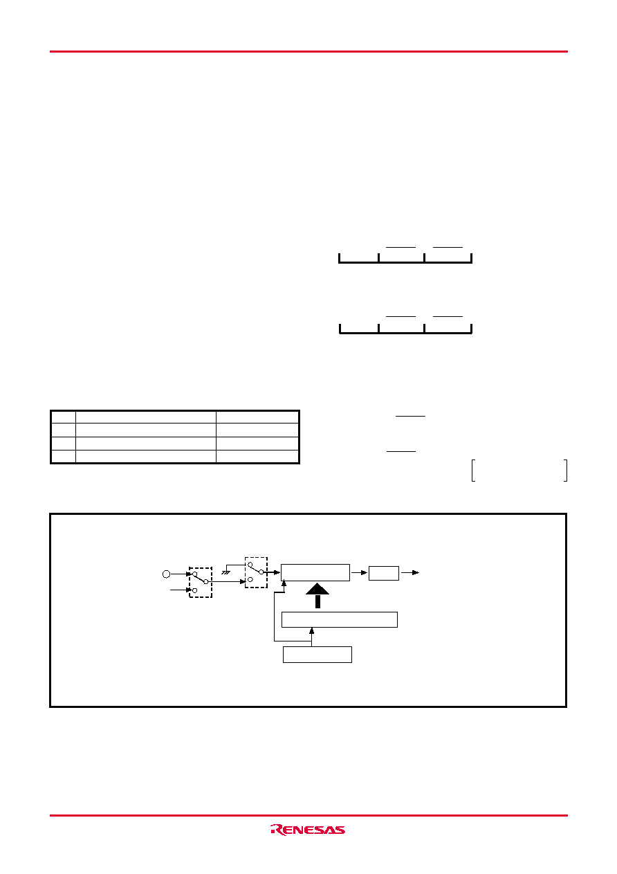
(2) LCD clock control
The LCD clock is determined by the timer LC count source selec-
tion bit (W62), timer LC control bit (W63), and timer LC.
Accordingly, the LCD clock frequency (F) is obtained by the follow-
ing formula. Numbers ( to ) shown below the formula
correspond to numbers in Figure 42, respectively.
When using the prescaler output (ORCLK) as timer LC count
source (W62=“1”)
F = ORCLK
When using the bit 4 of timer 5 as timer LC count source (W62=“0”)
F =
T54
[LC: 0 to 15]
The frame frequency and frame period for each display method
can be obtained by the following formula:
Frame frequency =
(Hz)
Frame period =
(s)
F: LCD clock frequency
1/n: Duty
Fig. 42 LCD clock control circuit structure
Duty
1/2
1/3
1/4
Used COM pins
COM0, COM1 (Note)
COM0–COM2 (Note)
COM0–COM3
Maximum number of displayed pixels
40 segments
60 segments
80 segments
Note: Leave unused COM pins open.
1
LC + 1
1
2
1
LC + 1
F
n
F
Note: Count source is stopped by setting “0” to this bit.
Timer LC
1/2
W63
0
1
(Note)
T54
W62
0
1
ORCLK
LCD clock
(4)
Reload register RLC
(4)
Register A
(TLCA)
1
2
相關(guān)PDF資料 |
PDF描述 |
|---|---|
| M34550E8FS | 4-BIT, UVPROM, 1.6 MHz, MICROCONTROLLER, CQCC80 |
| M34551E8-XXXFP | 4-BIT, OTPROM, MICROCONTROLLER, PQFP48 |
| M34554M8-XXXFP | 4-BIT, MROM, 6 MHz, MICROCONTROLLER, PQFP64 |
| M34554MC-XXXFP | 4-BIT, MROM, 6 MHz, MICROCONTROLLER, PQFP64 |
| M34571G6FP | 4-BIT, MROM, 6 MHz, MICROCONTROLLER, PDSO24 |
相關(guān)代理商/技術(shù)參數(shù) |
參數(shù)描述 |
|---|---|
| M3452-C09K1 | 制造商:Bonitron 功能描述:OVERVOLTAGE BRAKING TRANSISTOR |
| M3452-C125K2 | 制造商:Bonitron 功能描述:OVERVOLTAGE BRAKING TRANSISTOR |
| M3452-C125K2,A | 制造商:Bonitron 功能描述:OVERVOLTAGE BRAKING TRANSISTOR |
| M3452-C150B7 | 制造商:Bonitron 功能描述:OVERVOLTAGE BRAKING TRANSISTOR |
| M3452-C150B7-A | 制造商:Bonitron 功能描述:OVERVOLTAGE BRAKING TRANSISTOR |
發(fā)布緊急采購(gòu),3分鐘左右您將得到回復(fù)。