- 您現(xiàn)在的位置:買賣IC網(wǎng) > PDF目錄1974 > XCF128XFTG64C (Xilinx Inc)IC PROM SRL 128M GATE 64-FTBGA PDF資料下載
參數(shù)資料
| 型號: | XCF128XFTG64C |
| 廠商: | Xilinx Inc |
| 文件頁數(shù): | 17/88頁 |
| 文件大小: | 0K |
| 描述: | IC PROM SRL 128M GATE 64-FTBGA |
| 標(biāo)準(zhǔn)包裝: | 1 |
| 可編程類型: | 系統(tǒng)內(nèi)可編程 |
| 存儲容量: | 128Mb |
| 電源電壓: | 1.7 V ~ 2 V |
| 工作溫度: | -40°C ~ 85°C |
| 封裝/外殼: | 64-TBGA |
| 供應(yīng)商設(shè)備封裝: | 64-TFBGA |
| 包裝: | 托盤 |
| 產(chǎn)品目錄頁面: | 601 (CN2011-ZH PDF) |
| 其它名稱: | 122-1578 |
第1頁第2頁第3頁第4頁第5頁第6頁第7頁第8頁第9頁第10頁第11頁第12頁第13頁第14頁第15頁第16頁當(dāng)前第17頁第18頁第19頁第20頁第21頁第22頁第23頁第24頁第25頁第26頁第27頁第28頁第29頁第30頁第31頁第32頁第33頁第34頁第35頁第36頁第37頁第38頁第39頁第40頁第41頁第42頁第43頁第44頁第45頁第46頁第47頁第48頁第49頁第50頁第51頁第52頁第53頁第54頁第55頁第56頁第57頁第58頁第59頁第60頁第61頁第62頁第63頁第64頁第65頁第66頁第67頁第68頁第69頁第70頁第71頁第72頁第73頁第74頁第75頁第76頁第77頁第78頁第79頁第80頁第81頁第82頁第83頁第84頁第85頁第86頁第87頁第88頁
Platform Flash XL High-Density Configuration and Storage Device
DS617 (v3.0.1) January 07, 2010
Product Specification
24
R
Configuration Register
The Configuration Register is used to configure the type of bus access that the memory performs. Refer to "Read Modes,"
page 34 for details on read operations.
The Configuration Register is set through the Command Interface using the Set Configuration Register command. After a
reset or power-up, the device is configured for Synchronous Read (CR15 = 0). The Configuration Register bits (Table 12,
page 26) specify the selection of the burst length, burst type, burst X latency, and read operation. Refer to Figure 9, page 28
and Figure 10, page 30 for examples of synchronous burst configurations.
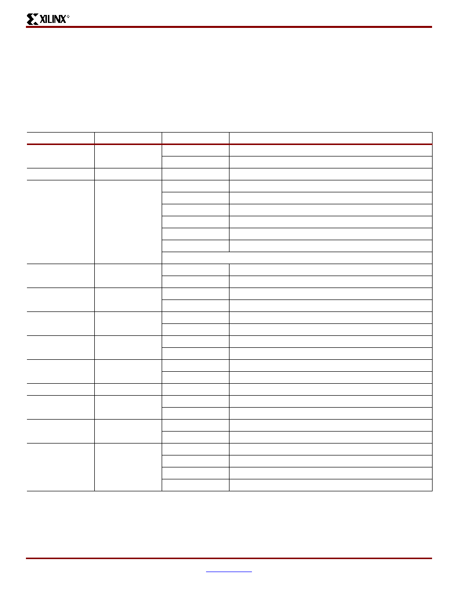
Table 12: Configuration Register Bits
Bits
Description
Value
Description
CR15
Read mode
0
Synchronous Read (default)
1
Asynchronous Read
CR14
Reserved
0
CR13–CR11
Clock Latency
010
2 clock latency(1)
011
3 clock latency
100
4 clock latency
101
5 clock latency
110
6 clock latency
111
7 clock latency (default)
Other configurations reserved
CR10
Wait Polarity
0
READY_WAIT with Wait function (CR4 = 0) is active Low
1
READY_WAIT with Wait function (CR4 = 0) is active High (default)
CR9
Data output
configuration
0
Data held for 1 clock cycle (default)
1
Data held for 2 clock cycles(1)
CR8
Wait Configuration
0
Wait active during wait state
1
Wait active 1 clock cycle before wait state (default)
CR7
Burst Type
0
Reserved
1
Sequential (default)
CR6
Valid Clock Edge
0
Falling clock edge
1
Rising clock edge (default)
CR5
Reserved
0
–
CR4
Device_ready
0
READY_WAIT signal has the Wait function
1
READY_WAIT signal has the Ready function (default)
CR3(2)
Wrap burst
0
Wrap
1
No wrap (default)
CR2–CR0(2)
Burst Length
001
4 words
010
8 words
011
16 words
111
Continuous (default)
Notes:
1.
The combination X-Latency = 2, Data held for two clock cycles and Wait active one data cycle before the WAIT state is not supported.
2.
CR3 (wrap/no wrap) bit has no effect when CR2-CR0 (burst length) bits are set to continuous burst mode. Platform Flash XL wraps to the first
memory address after the device outputs the data from the last memory address.
相關(guān)PDF資料 |
PDF描述 |
|---|---|
| XCF32PFS48C | IC PROM SRL 1.8V 32M 48CSBGA |
| XCR3256XL-7CS280C | IC CPLD 256MCELL 3.3V HP 280CSP |
| XCS10-3VQG100C | IC FPGA 5V C-TEMP 100-VQFP |
| XCV600E-8HQ240C | IC FPGA 1.8V C-TEMP 240-HQFP |
| XCV812E-8FG900C | IC FPGA 1.8V C-TEMP 900-FBGA |
相關(guān)代理商/技術(shù)參數(shù) |
參數(shù)描述 |
|---|---|
| XCF128XFTG64CES | 制造商:Xilinx 功能描述: |
| XCF12-L4Z1 | 制造商:SAIA - BURGESS ELECTRONICS INC. 功能描述:Catalogue / XCF12-L4Z1 |
| XCF12-S1 | 制造商:SAIA - BURGESS ELECTRONICS INC. 功能描述:Catalogue / XCF12-S1 |
| XCF13-S1 | 制造商:SAIA - BURGESS ELECTRONICS INC. 功能描述:Catalogue / XCF13-S1 |
| XCF16P | 制造商:XILINX 制造商全稱:XILINX 功能描述:Platform Flash In-System Programmable Configuration PROMs |
發(fā)布緊急采購,3分鐘左右您將得到回復(fù)。