- 您現(xiàn)在的位置:買賣IC網(wǎng) > PDF目錄383740 > PFR4200MAE40 (飛思卡爾半導體(中國)有限公司) FlexRay Communication Controllers PDF資料下載
參數(shù)資料
| 型號: | PFR4200MAE40 |
| 廠商: | 飛思卡爾半導體(中國)有限公司 |
| 英文描述: | FlexRay Communication Controllers |
| 中文描述: | FlexRay通信控制器 |
| 文件頁數(shù): | 34/260頁 |
| 文件大?。?/td> | 1782K |
| 代理商: | PFR4200MAE40 |
第1頁第2頁第3頁第4頁第5頁第6頁第7頁第8頁第9頁第10頁第11頁第12頁第13頁第14頁第15頁第16頁第17頁第18頁第19頁第20頁第21頁第22頁第23頁第24頁第25頁第26頁第27頁第28頁第29頁第30頁第31頁第32頁第33頁當前第34頁第35頁第36頁第37頁第38頁第39頁第40頁第41頁第42頁第43頁第44頁第45頁第46頁第47頁第48頁第49頁第50頁第51頁第52頁第53頁第54頁第55頁第56頁第57頁第58頁第59頁第60頁第61頁第62頁第63頁第64頁第65頁第66頁第67頁第68頁第69頁第70頁第71頁第72頁第73頁第74頁第75頁第76頁第77頁第78頁第79頁第80頁第81頁第82頁第83頁第84頁第85頁第86頁第87頁第88頁第89頁第90頁第91頁第92頁第93頁第94頁第95頁第96頁第97頁第98頁第99頁第100頁第101頁第102頁第103頁第104頁第105頁第106頁第107頁第108頁第109頁第110頁第111頁第112頁第113頁第114頁第115頁第116頁第117頁第118頁第119頁第120頁第121頁第122頁第123頁第124頁第125頁第126頁第127頁第128頁第129頁第130頁第131頁第132頁第133頁第134頁第135頁第136頁第137頁第138頁第139頁第140頁第141頁第142頁第143頁第144頁第145頁第146頁第147頁第148頁第149頁第150頁第151頁第152頁第153頁第154頁第155頁第156頁第157頁第158頁第159頁第160頁第161頁第162頁第163頁第164頁第165頁第166頁第167頁第168頁第169頁第170頁第171頁第172頁第173頁第174頁第175頁第176頁第177頁第178頁第179頁第180頁第181頁第182頁第183頁第184頁第185頁第186頁第187頁第188頁第189頁第190頁第191頁第192頁第193頁第194頁第195頁第196頁第197頁第198頁第199頁第200頁第201頁第202頁第203頁第204頁第205頁第206頁第207頁第208頁第209頁第210頁第211頁第212頁第213頁第214頁第215頁第216頁第217頁第218頁第219頁第220頁第221頁第222頁第223頁第224頁第225頁第226頁第227頁第228頁第229頁第230頁第231頁第232頁第233頁第234頁第235頁第236頁第237頁第238頁第239頁第240頁第241頁第242頁第243頁第244頁第245頁第246頁第247頁第248頁第249頁第250頁第251頁第252頁第253頁第254頁第255頁第256頁第257頁第258頁第259頁第260頁
Device Overview
MFR4200 Data Sheet, Rev. 0
34
Freescale Semiconductor
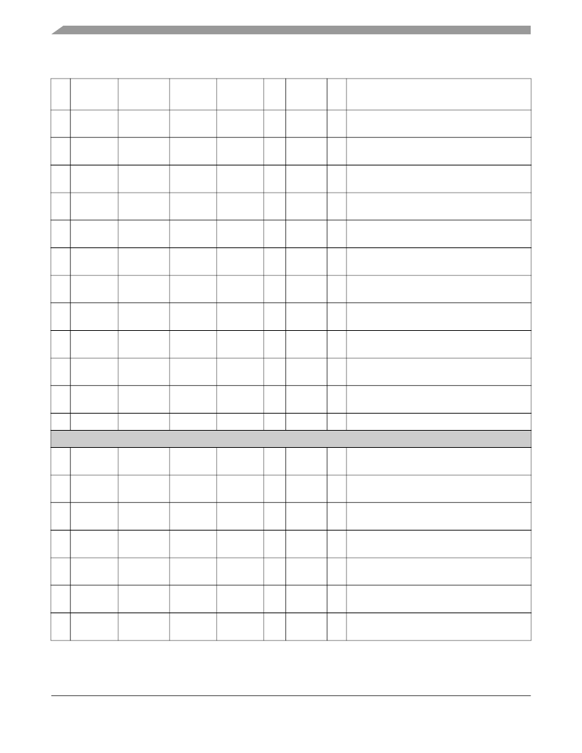
62
D8
PAD7
-
VDDX
I/O
Z/DC/PC
Z
AMI data bus / HCS12 multiplexed address/data
bus.
61
D7
PAD8
-
VDDX
I/O
Z/DC/PC
Z
AMI data bus / HCS12 multiplexed address/data
bus.
58
D6
PAD9
-
VDDX
I/O
Z/DC/PC
Z
AMI data bus / HCS12 multiplexed address/data
bus.
57
D5
PAD10
-
VDDX
I/O
Z/DC/PC
Z
AMI data bus / HCS12 multiplexed address/data
bus.
56
D4
PAD11
-
VDDX
I/O
Z/DC/PC
Z
AMI data bus / HCS12 multiplexed address/data
bus.
55
D3
PAD12
-
VDDX
I/O
Z/DC/PC
Z
AMI data bus / HCS12 multiplexed address/data
bus.
51
D2
PAD13
-
VDDX
I/O
Z/DC/PC
Z
AMI data bus / HCS12 multiplexed address/data
bus.
40
D1
PAD14
-
VDDX
I/O
Z/DC/PC
Z
AMI data bus / HCS12 multiplexed address/data
bus.
39
D0
PAD15
-
VDDX
I/O
Z/DC/PC
Z
AMI data bus / HCS12 multiplexed address/data
bus. D0 is the LSB of the AMI data bus
29
CE#
LSTRB
-
VDDX
I
PC
-
AMI chip select signal / HCS12 low-byte strobe
signal
30
WE#
RW_CC#
-
VDDX
I
PC
-
AMI write enable signal/ HCS12 read/write
select signal
52
ECLK_CC
-
-
VDDX
I
PC
-
HCS12 clock input
Physical Layer Interface
32
BGT
DBG2
IF_SEL0
VDDX
I/O
DC/PD
-
Bus Guardian Tick / Debug strobe point signal
2/Host interface selection 0
48
MT
CLK_S1
-
VDDX
I/O
DC/PD
-
Bus Guardian Macrotick/Controller clock output
select signal 1
47
ARM
DBG1
CLK_S0
VDDX
I/O
DC/PD
-
Bus Guardian ARM signal / Debug strobe point
signal1/Controller clock output select signal 0
33
RXD_BG1
RXD2_485
-
VDDX
I
PC
-
PHY Data receiver input / RS485 Data receiver
input
43
RXD_BG2
RXD2_485
-
VDDX
I
PC
-
PHY Data receiver input / RS485 Data receiver
input
36
TXEN1#
TXE1_485#
-
VDDX
O
DC
1
Transmit enable for PHY / Transmit enable for
RS485
44
TXEN2#
TXE2_485#
-
VDDX
O
DC
1
Transmit enable for PHY / Transmit enable for
RS485
Table 2-7. Pin Functions and Signal Properties (continued)
Pin
N
Pin
1
Function1
Pin
1
Function2
Pin
1
Function3
Powered
by
In/
Out
Pin
type
2,3
Re
set
Functional Description
相關(guān)PDF資料 |
PDF描述 |
|---|---|
| PFR4200MPB40 | FlexRay Communication Controllers |
| PFR850S | FAST RECOVERY RECTIFIER DIODES |
| PFR851S | FAST RECOVERY RECTIFIER DIODES |
| PFR852S | FAST RECOVERY RECTIFIER DIODES |
| PFR853S | FAST RECOVERY RECTIFIER DIODES |
相關(guān)代理商/技術(shù)參數(shù) |
參數(shù)描述 |
|---|---|
| PFR4200MPB40 | 制造商:FREESCALE 制造商全稱:Freescale Semiconductor, Inc 功能描述:FlexRay Communication Controllers |
| PFR4310E1MAE40 | 制造商:Freescale Semiconductor 功能描述: |
| PFR4KR100E | 制造商:OHMITE 制造商全稱:Ohmite Mfg. Co. 功能描述:Powr-Rib Edgewound Edgewound and Round Wire |
| PFR5 102J630J11L4 | 制造商:Evox Rifa / KEMET 功能描述:PULSE CAP 0.001UF 630VDC |
| PFR5 102J63J11L4 | 制造商:Evox Rifa / KEMET 功能描述:PULSE CAP 0.001UF 63VDC |
發(fā)布緊急采購,3分鐘左右您將得到回復。