- 您現(xiàn)在的位置:買賣IC網 > PDF目錄383724 > ORT8850 Field-Programmable System Chip (FPSC) Eight-Channel x 850 Mbits/s Backplane Transceiver PDF資料下載
參數(shù)資料
| 型號: | ORT8850 |
| 英文描述: | Field-Programmable System Chip (FPSC) Eight-Channel x 850 Mbits/s Backplane Transceiver |
| 中文描述: | 現(xiàn)場可編程系統(tǒng)芯片(促進文化基金)8通道x 850 Mbits /秒背板收發(fā)器 |
| 文件頁數(shù): | 46/112頁 |
| 文件大?。?/td> | 2417K |
| 代理商: | ORT8850 |
第1頁第2頁第3頁第4頁第5頁第6頁第7頁第8頁第9頁第10頁第11頁第12頁第13頁第14頁第15頁第16頁第17頁第18頁第19頁第20頁第21頁第22頁第23頁第24頁第25頁第26頁第27頁第28頁第29頁第30頁第31頁第32頁第33頁第34頁第35頁第36頁第37頁第38頁第39頁第40頁第41頁第42頁第43頁第44頁第45頁當前第46頁第47頁第48頁第49頁第50頁第51頁第52頁第53頁第54頁第55頁第56頁第57頁第58頁第59頁第60頁第61頁第62頁第63頁第64頁第65頁第66頁第67頁第68頁第69頁第70頁第71頁第72頁第73頁第74頁第75頁第76頁第77頁第78頁第79頁第80頁第81頁第82頁第83頁第84頁第85頁第86頁第87頁第88頁第89頁第90頁第91頁第92頁第93頁第94頁第95頁第96頁第97頁第98頁第99頁第100頁第101頁第102頁第103頁第104頁第105頁第106頁第107頁第108頁第109頁第110頁第111頁第112頁
46
Agere Systems Inc.
Data Sheet
August 2001
Eight-Channel x 850 Mbits/s Backplane Transceiver
ORCA
ORT8850 FPSC
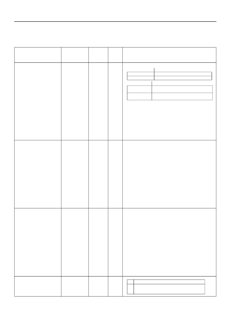
Memory Map
(continued)
Table 12. Memory Map Descriptions
(continued)
Bit/Register Name(S)
Bit/ Register
Location
(Hex)
09 [0]
Register
Type
Reset
Value
(Hex)
1
1
1
1
Description
serial port output MUX
select for ch#1
serial port output MUX
select for ch#3
parallel port output MUX
select for ch#1
parallel port output MUX
select for ch#3
serial port output MUX
select for ch#5
parallel port output MUX
select for ch#7
serial port output MUX
select for ch#5
parallel port output MUX
select for ch#7
FIFO aligner threshold
value (min) Default = 2
FIFO aligner threshold
value (max) Default = 15
09 [1]
09 [2]
09 [3]
09 [4]
09 [5]
09 [6]
09 [7]
creg
0A [0:4]
0B [0:4]
creg
40
A8
These are the minimum and maximum thresholds
values for the per channel receive direction align-
ment FIFOs. If and when the minimum or maximum
threshold value is violated by a particular channel,
then the interrupt event
“
FIFO aligner threshold
error
”
will be generated for that channel and latched
as a
“
FIFO aligner threshold error flag
”
in the
respective per STS-12 interrupt alarm register.
The allowable range for minimum threshold values
is 1 to 23.
The allowable range for maximum threshold values
is 0 to 22.
Note that the minimum and maximum FIFO aligner
threshold values apply to all four channels.
These three per device control signals are used in
conjunction with the per channel
“
a1 a2 error insert
command
”
control bits to force A1 A2 errors in the
transmit direction.
If a particular channel
’
s
“
a1 a2 error insert com-
mand
”
control bit is set to the value 1 then the
“
A1
and A2 error insert values
”
will be inserted into that
channels respective A1 and A2 bytes. The number
of consecutive frames to be corrupted is deter-
mined by the
“
number of consecutive A1 A2 errors
to generate[0:3]
”
control bits.
The error insertion is based on a rising edge detec-
tor. As such the control must be set to value 0
before trying to initiate a second a1 a2 corruption.
0
No loopback.
number of consecutive
A1 A2 errors to generate
[0:3]
A1 error insert value
[0:7]
A2 error insert value
[0:7]
0C [0:3]
0D [0:7]
0E [0:7]
creg
00
00
00
backplane side loop-
back control
0C [4]
creg
0
serial port output MUX
0
1
TOH output is multiplexed to next channel.
TOH output is multiplexed to same channel.
parallel port output
0
Parallel output data bus is multiplexed to
next channel.
1
Parallel output data bus is multiplexed to
same channel
1
rx to tx loopback on backplane side. Serial input is run through
SERDES and looped back in parallel to SERDES and out
serial.
相關PDF資料 |
PDF描述 |
|---|---|
| ORT8850H | Field-Programmable System Chip (FPSC) Eight-Channel x 850 Mbits/s Backplane Transceiver |
| ORT8850L | Field-Programmable System Chip (FPSC) Eight-Channel x 850 Mbits/s Backplane Transceiver |
| OS1001 | Interface IC |
| OS1010 | Optoelectronic |
| OS1011 | SINGLE 1.8V, 200 KHZ OP, E TEMP, -40C to +125C, 8-PDIP, TUBE |
相關代理商/技術參數(shù) |
參數(shù)描述 |
|---|---|
| ORT8850-FPSC-EV | 功能描述:可編程邏輯 IC 開發(fā)工具 ORCA ORT8850 FPSC Eval Brd RoHS:否 制造商:Altera Corporation 產品:Development Kits 類型:FPGA 工具用于評估:5CEFA7F3 接口類型: 工作電源電壓: |
| ORT8850H | 制造商:AGERE 制造商全稱:AGERE 功能描述:Field-Programmable System Chip (FPSC) Eight-Channel x 850 Mbits/s Backplane Transceiver |
| ORT8850H-1BM680C | 功能描述:FPGA - 現(xiàn)場可編程門陣列 16192 LUT 297 I/O RoHS:否 制造商:Altera Corporation 系列:Cyclone V E 柵極數(shù)量: 邏輯塊數(shù)量:943 內嵌式塊RAM - EBR:1956 kbit 輸入/輸出端數(shù)量:128 最大工作頻率:800 MHz 工作電源電壓:1.1 V 最大工作溫度:+ 70 C 安裝風格:SMD/SMT 封裝 / 箱體:FBGA-256 |
| ORT8850H-1BM680I | 功能描述:FPGA - 現(xiàn)場可編程門陣列 16192 LUT 297 I/O RoHS:否 制造商:Altera Corporation 系列:Cyclone V E 柵極數(shù)量: 邏輯塊數(shù)量:943 內嵌式塊RAM - EBR:1956 kbit 輸入/輸出端數(shù)量:128 最大工作頻率:800 MHz 工作電源電壓:1.1 V 最大工作溫度:+ 70 C 安裝風格:SMD/SMT 封裝 / 箱體:FBGA-256 |
| ORT8850H-1BMN680C | 功能描述:FPGA - 現(xiàn)場可編程門陣列 16192 LUT 297 I/O RoHS:否 制造商:Altera Corporation 系列:Cyclone V E 柵極數(shù)量: 邏輯塊數(shù)量:943 內嵌式塊RAM - EBR:1956 kbit 輸入/輸出端數(shù)量:128 最大工作頻率:800 MHz 工作電源電壓:1.1 V 最大工作溫度:+ 70 C 安裝風格:SMD/SMT 封裝 / 箱體:FBGA-256 |
發(fā)布緊急采購,3分鐘左右您將得到回復。