- 您現(xiàn)在的位置:買賣IC網(wǎng) > PDF目錄180243 > M7A3PE600-FFG484I FPGA, 600000 GATES, PBGA484 PDF資料下載
參數(shù)資料
| 型號(hào): | M7A3PE600-FFG484I |
| 元件分類: | FPGA |
| 英文描述: | FPGA, 600000 GATES, PBGA484 |
| 封裝: | 1 MM PITCH, FBGA-484 |
| 文件頁(yè)數(shù): | 99/168頁(yè) |
| 文件大小: | 1335K |
| 代理商: | M7A3PE600-FFG484I |
第1頁(yè)第2頁(yè)第3頁(yè)第4頁(yè)第5頁(yè)第6頁(yè)第7頁(yè)第8頁(yè)第9頁(yè)第10頁(yè)第11頁(yè)第12頁(yè)第13頁(yè)第14頁(yè)第15頁(yè)第16頁(yè)第17頁(yè)第18頁(yè)第19頁(yè)第20頁(yè)第21頁(yè)第22頁(yè)第23頁(yè)第24頁(yè)第25頁(yè)第26頁(yè)第27頁(yè)第28頁(yè)第29頁(yè)第30頁(yè)第31頁(yè)第32頁(yè)第33頁(yè)第34頁(yè)第35頁(yè)第36頁(yè)第37頁(yè)第38頁(yè)第39頁(yè)第40頁(yè)第41頁(yè)第42頁(yè)第43頁(yè)第44頁(yè)第45頁(yè)第46頁(yè)第47頁(yè)第48頁(yè)第49頁(yè)第50頁(yè)第51頁(yè)第52頁(yè)第53頁(yè)第54頁(yè)第55頁(yè)第56頁(yè)第57頁(yè)第58頁(yè)第59頁(yè)第60頁(yè)第61頁(yè)第62頁(yè)第63頁(yè)第64頁(yè)第65頁(yè)第66頁(yè)第67頁(yè)第68頁(yè)第69頁(yè)第70頁(yè)第71頁(yè)第72頁(yè)第73頁(yè)第74頁(yè)第75頁(yè)第76頁(yè)第77頁(yè)第78頁(yè)第79頁(yè)第80頁(yè)第81頁(yè)第82頁(yè)第83頁(yè)第84頁(yè)第85頁(yè)第86頁(yè)第87頁(yè)第88頁(yè)第89頁(yè)第90頁(yè)第91頁(yè)第92頁(yè)第93頁(yè)第94頁(yè)第95頁(yè)第96頁(yè)第97頁(yè)第98頁(yè)當(dāng)前第99頁(yè)第100頁(yè)第101頁(yè)第102頁(yè)第103頁(yè)第104頁(yè)第105頁(yè)第106頁(yè)第107頁(yè)第108頁(yè)第109頁(yè)第110頁(yè)第111頁(yè)第112頁(yè)第113頁(yè)第114頁(yè)第115頁(yè)第116頁(yè)第117頁(yè)第118頁(yè)第119頁(yè)第120頁(yè)第121頁(yè)第122頁(yè)第123頁(yè)第124頁(yè)第125頁(yè)第126頁(yè)第127頁(yè)第128頁(yè)第129頁(yè)第130頁(yè)第131頁(yè)第132頁(yè)第133頁(yè)第134頁(yè)第135頁(yè)第136頁(yè)第137頁(yè)第138頁(yè)第139頁(yè)第140頁(yè)第141頁(yè)第142頁(yè)第143頁(yè)第144頁(yè)第145頁(yè)第146頁(yè)第147頁(yè)第148頁(yè)第149頁(yè)第150頁(yè)第151頁(yè)第152頁(yè)第153頁(yè)第154頁(yè)第155頁(yè)第156頁(yè)第157頁(yè)第158頁(yè)第159頁(yè)第160頁(yè)第161頁(yè)第162頁(yè)第163頁(yè)第164頁(yè)第165頁(yè)第166頁(yè)第167頁(yè)第168頁(yè)
ProASIC3E Flash Family FPGAs
2- 24
Advanced v0.5
Signal Descriptions for RAM4K9
The following signals are used to configure the RAM4K9
memory element:
WIDTHA and WIDTHB
These signals enable the RAM to be configured in one of
four allowable aspect ratios (Table 2-5).
BLKA and BLKB
These signals are active low and will enable the
respective ports when asserted. When a BLKx signal is
deasserted, that port’s outputs hold the previous value.
WENA and WENB
These signals switch the RAM between read and write
modes for the respective ports. A low on these signals
indicates a write operation, and a high indicates a read.
CLKA and CLKB
These are the clock signals for the synchronous read and
write operations. These can be driven independently or
with the same driver.
PIPEA and PIPEB
These signals are used to specify pipelined read on the
output. A low on PIPEA or PIPEB indicates a nonpipelined
read, and the data appears on the corresponding output
in the same clock cycle. A high indicates a pipelined read,
and data appears on the corresponding output in the
next clock cycle.
WMODEA and WMODEB
These signals are used to configure the behavior of the
output when RAM is in the write mode. A low on these
signals makes the output retain data from the previous
read. A high indicates pass-through behavior, wherein
the data being written will appear immediately on the
output. This signal is overridden when the RAM is being
read.
RESET
This active low signal resets the control logic and forces
the output hold state registers to zero when asserted. It
does not reset the contents of the memory array.
While the RESET signal is active, read and write
operations are disabled. As with any asynchronous reset
signal, care must be taken not to assert it too close to the
edges of active read and write clocks. Refer to the tables
beginning
with
for
the
specifications.
ADDRA and ADDRB
These are used as read or write addresses, and they are 12
bits wide. When a depth of less than 4 k is specified, the
unused high-order bits must be grounded (Table 2-6).
DINA and DINB
These are the input data signals, and they are nine bits
wide. Not all nine bits are valid in all configurations.
When a data width less than nine is specified, unused
high-order signals must be grounded (Table 2-7).
DOUTA and DOUTB
These are the nine-bit output data signals. Not all nine
bits are valid in all configurations. As with DINA and
DINB, high-order bits may not be used (Table 2-7). The
output data on unused pins is undefined.
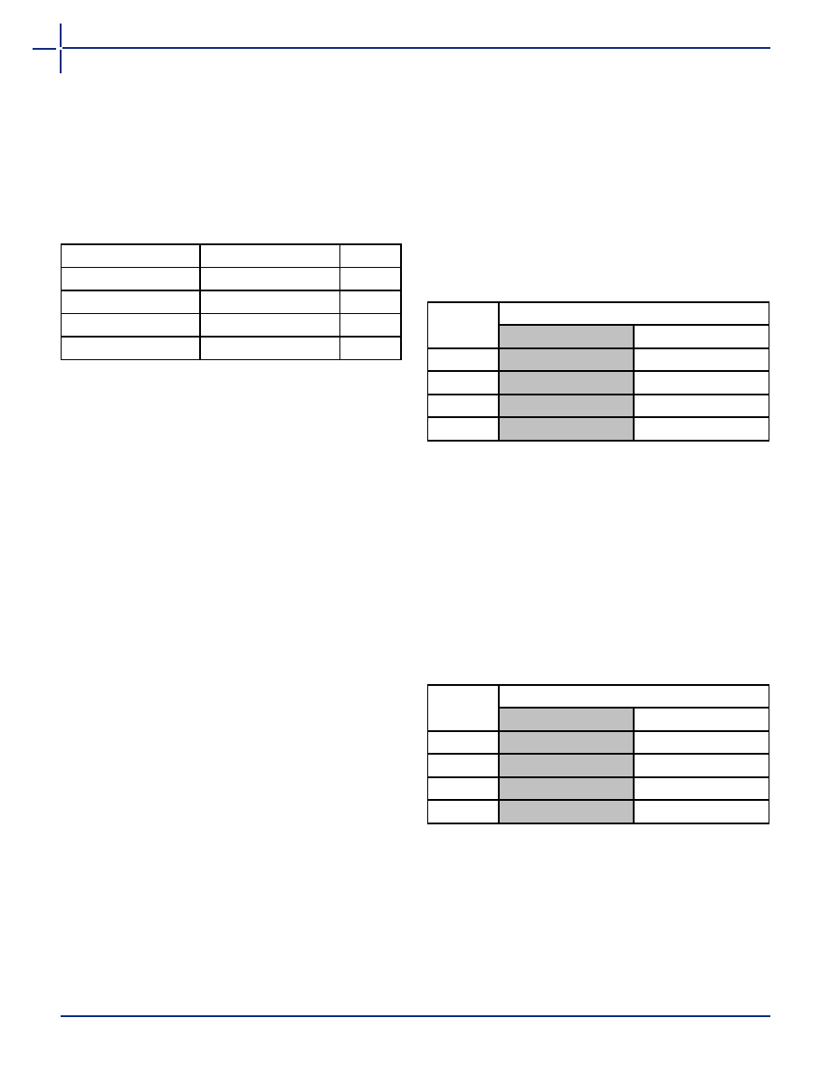
Table 2-5 Allowable Aspect Ratio Settings for
WIDTHA[1:0]
WIDTHA[1:0]
WIDTHB[1:0]
DxW
00
4kx1
01
2kx2
10
1kx4
11
512x9
Note: The aspect ratio settings are constant and cannot be
changed on-the-fly.
Table 2-6 Address Pins Unused/Used for Various
Supported Bus Widths
DxW
ADDRx
Unused
Used
4kx1
None
[11:0]
2kx2
[11]
[10:0]
1kx4
[11:10]
[9:0]
512x9
[11:9]
[8:0]
Note: The "x" in ADDRx implies A or B.
Table 2-7 Unused/Used Input and Output Data Pins for
Various Supported Bus Widths
DxW
DINx/DOUTx
Unused
Used
4kx1
[8:1]
[0]
2kx2
[8:2]
[1:0]
1kx4
[8:4]
[3:0]
512x9
None
[8:0]
Note: The "x" in DINx or DOUTx implies A or B.
相關(guān)PDF資料 |
PDF描述 |
|---|---|
| M7A3PE600-FFGG256I | FPGA, 600000 GATES, PBGA256 |
| M7A3PE600-FFGG484I | FPGA, 600000 GATES, PBGA484 |
| M7A3PE600-FPQ208I | FPGA, 600000 GATES, PQFP208 |
| M7A3PE600-FPQG208I | FPGA, 600000 GATES, PQFP208 |
| M7R-R63FAJFREQ | CRYSTAL OSCILLATOR, CLOCK, 80.001 MHz - 125 MHz, CMOS/TTL OUTPUT |
相關(guān)代理商/技術(shù)參數(shù) |
參數(shù)描述 |
|---|---|
| M7A5 | 制造商:未知廠家 制造商全稱:未知廠家 功能描述:MEDIUM CURRENT SILICON RECTIFIERS |
| M7A9 | 制造商:未知廠家 制造商全稱:未知廠家 功能描述:MEDIUM CURRENT SILICON RECTIFIERS |
| M7AFS600-1FG256 | 制造商:Microsemi Corporation 功能描述:FPGA FUSION 600K GATES 1282.05MHZ 130NM 1.5V 256FBGA - Trays 制造商:Microsemi SOC Products Group 功能描述:FPGA FUSION 600K GATES 1282.05MHZ 130NM 1.5V 256FBGA - Trays |
| M7AFS600-1FG256ES | 制造商:ACTEL 制造商全稱:Actel Corporation 功能描述:Actel Fusion Mixed-Signal FPGAs |
| M7AFS600-1FG256I | 制造商:Microsemi Corporation 功能描述:FPGA FUSION 600K GATES 1282.05MHZ 130NM 1.5V 256FBGA - Trays 制造商:Microsemi SOC Products Group 功能描述:FPGA FUSION 600K GATES 1282.05MHZ 130NM 1.5V 256FBGA - Trays |
發(fā)布緊急采購(gòu),3分鐘左右您將得到回復(fù)。