- 您現(xiàn)在的位置:買賣IC網(wǎng) > PDF目錄180243 > M7A3PE600-FFG484I FPGA, 600000 GATES, PBGA484 PDF資料下載
參數(shù)資料
| 型號(hào): | M7A3PE600-FFG484I |
| 元件分類: | FPGA |
| 英文描述: | FPGA, 600000 GATES, PBGA484 |
| 封裝: | 1 MM PITCH, FBGA-484 |
| 文件頁(yè)數(shù): | 113/168頁(yè) |
| 文件大?。?/td> | 1335K |
| 代理商: | M7A3PE600-FFG484I |
第1頁(yè)第2頁(yè)第3頁(yè)第4頁(yè)第5頁(yè)第6頁(yè)第7頁(yè)第8頁(yè)第9頁(yè)第10頁(yè)第11頁(yè)第12頁(yè)第13頁(yè)第14頁(yè)第15頁(yè)第16頁(yè)第17頁(yè)第18頁(yè)第19頁(yè)第20頁(yè)第21頁(yè)第22頁(yè)第23頁(yè)第24頁(yè)第25頁(yè)第26頁(yè)第27頁(yè)第28頁(yè)第29頁(yè)第30頁(yè)第31頁(yè)第32頁(yè)第33頁(yè)第34頁(yè)第35頁(yè)第36頁(yè)第37頁(yè)第38頁(yè)第39頁(yè)第40頁(yè)第41頁(yè)第42頁(yè)第43頁(yè)第44頁(yè)第45頁(yè)第46頁(yè)第47頁(yè)第48頁(yè)第49頁(yè)第50頁(yè)第51頁(yè)第52頁(yè)第53頁(yè)第54頁(yè)第55頁(yè)第56頁(yè)第57頁(yè)第58頁(yè)第59頁(yè)第60頁(yè)第61頁(yè)第62頁(yè)第63頁(yè)第64頁(yè)第65頁(yè)第66頁(yè)第67頁(yè)第68頁(yè)第69頁(yè)第70頁(yè)第71頁(yè)第72頁(yè)第73頁(yè)第74頁(yè)第75頁(yè)第76頁(yè)第77頁(yè)第78頁(yè)第79頁(yè)第80頁(yè)第81頁(yè)第82頁(yè)第83頁(yè)第84頁(yè)第85頁(yè)第86頁(yè)第87頁(yè)第88頁(yè)第89頁(yè)第90頁(yè)第91頁(yè)第92頁(yè)第93頁(yè)第94頁(yè)第95頁(yè)第96頁(yè)第97頁(yè)第98頁(yè)第99頁(yè)第100頁(yè)第101頁(yè)第102頁(yè)第103頁(yè)第104頁(yè)第105頁(yè)第106頁(yè)第107頁(yè)第108頁(yè)第109頁(yè)第110頁(yè)第111頁(yè)第112頁(yè)當(dāng)前第113頁(yè)第114頁(yè)第115頁(yè)第116頁(yè)第117頁(yè)第118頁(yè)第119頁(yè)第120頁(yè)第121頁(yè)第122頁(yè)第123頁(yè)第124頁(yè)第125頁(yè)第126頁(yè)第127頁(yè)第128頁(yè)第129頁(yè)第130頁(yè)第131頁(yè)第132頁(yè)第133頁(yè)第134頁(yè)第135頁(yè)第136頁(yè)第137頁(yè)第138頁(yè)第139頁(yè)第140頁(yè)第141頁(yè)第142頁(yè)第143頁(yè)第144頁(yè)第145頁(yè)第146頁(yè)第147頁(yè)第148頁(yè)第149頁(yè)第150頁(yè)第151頁(yè)第152頁(yè)第153頁(yè)第154頁(yè)第155頁(yè)第156頁(yè)第157頁(yè)第158頁(yè)第159頁(yè)第160頁(yè)第161頁(yè)第162頁(yè)第163頁(yè)第164頁(yè)第165頁(yè)第166頁(yè)第167頁(yè)第168頁(yè)
ProASIC3E Flash Family FPGAs
A d v an c ed v0 . 5
2-37
Grounds
Powers
I/Os and other pins
Cold-Sparing Support
Cold-sparing means that a subsystem with no power
applied (usually a circuit board) is electrically connected
to the system that is in operation. This means that all
input buffers of the subsystem must present very high
input impedance with no power applied so as not to
disturb the operating portion of the system.
ProASIC3E devices support cold-sparing for all I/O
configurations. Standards such as PCI which require I/O
clamp diodes can also achieve cold-sparing compliance,
since clamp diodes get disconnected internally when the
supplies are at 0 V.
If the resistor is chosen, the resistor value must be
calculated based on decoupling capacitance on a given
power supply on the board (this decoupling capacitor is
in parallel with this resistor). The RC time constant
should ensure full discharge of supplies before cold-
sparing functionality is required. The resistor is necessary
to ensure that the power pins are discharged to ground
every time there is an interruption of power to the
device.
Electrostatic Discharge (ESD) Protection
ProASIC3E devices are tested per JEDEC Standard
JESD22-A114-B.
ProASIC3E devices contain clamp diodes at every I/O,
global, and power pad. Clamp diodes protect all device
pads against damage from ESD as well as from excessive
voltage transients.
ProASIC3E devices are tested to the following models:
Human Body Model (HBM) with a tolerance of 2,000 V,
the Machine Model (MM) with a tolerance of 250 V, and
the Charged Device Model (CDM) with a tolerance of
200 V.
Each I/O has two clamp diodes. One diode has its
positive (P) side connected to the pad and its negative
(N) side connected to VCCI. The second diode has its P
side connected to GND, and its N side connected to the
pad. During operation, these diodes are normally
biased in the Off state, except when transient voltage is
significantly above VCCI or below GND levels.
By selecting the appropriate I/O configuration, the diode
is turned on or off. Refer to Table 2-18 for more
information about the I/O standards and the clamp
diode.
The second diode is always connected to the pad,
regardless of the I/O configuration selected.
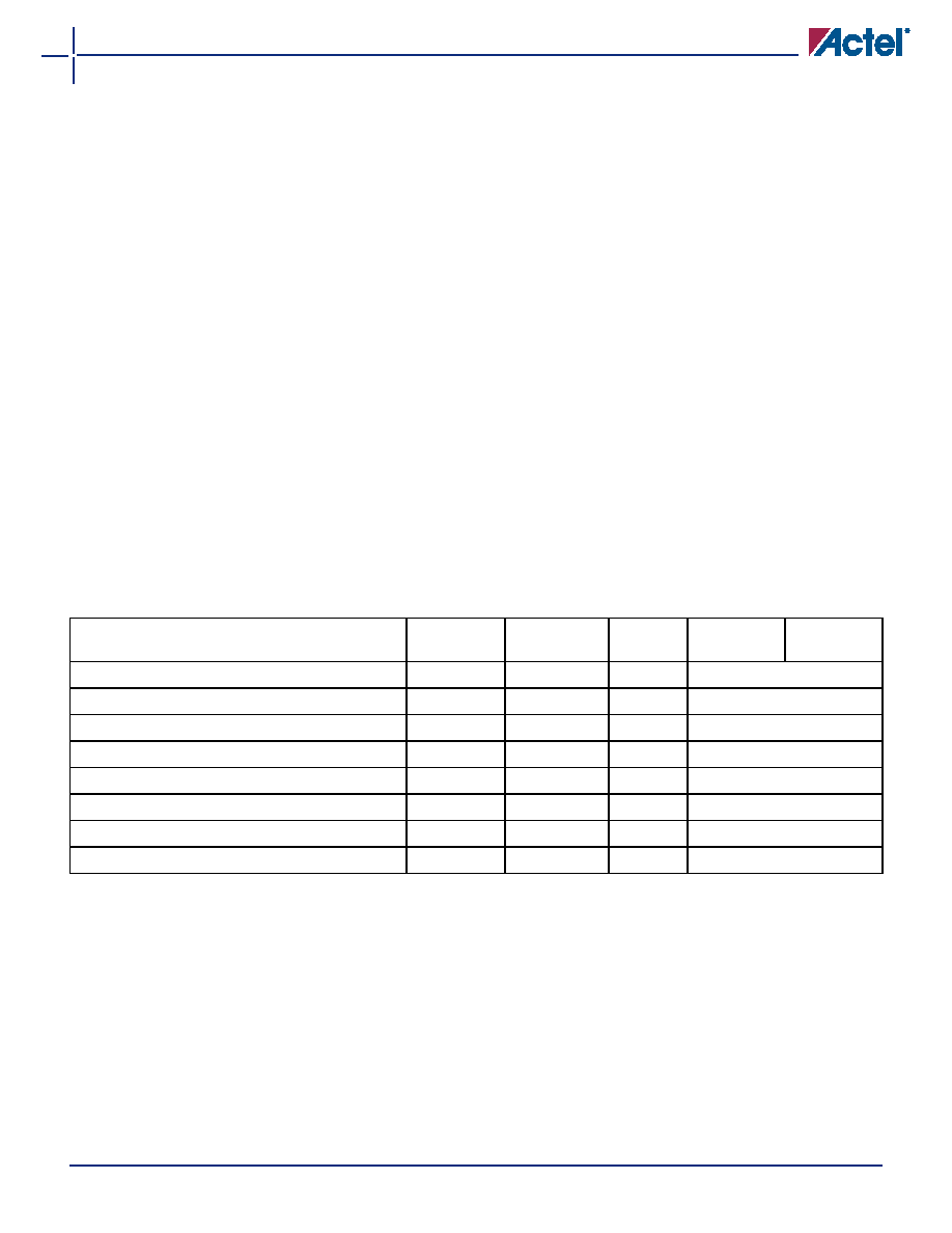
Table 2-18 I/O Hot-Swap and 5 V Input Tolerance Capabilities
I/O Assignment
Clamp
Diode
Hot
Insertion
5 V Input
Tolerance Input Buffer
Output
Buffer
3.3 V LVTTL/LVCMOS
No
Yes
Yes1
Enabled/Disabled
3.3 V PCI, 3.3 V PCI-X
Yes
No
Yes1
Enabled/Disabled
LVCMOS 2.5 V 3
No
Yes
No
Enabled/Disabled
LVCMOS 2.5 V / 5.0 V 3
Yes
No
Yes2
Enabled/Disabled
LVCMOS 1.8 V
No
Yes
No
Enabled/Disabled
LVCMOS 1.5 V
No
Yes
No
Enabled/Disabled
Voltage-Referenced Input Buffer
No
Yes
No
Enabled/Disabled
Differential, LVDS/BLVDS/M-LVDS/LVPECL
No
Yes
No
Enabled/Disabled
Notes:
1. Can be implemented with an external IDT bus switch, resistor divider, or zener with resistor.
2. Can be implemented with an external resistor and an internal clamp diode.
3. In the SmartGen Core Reference Guide, select the LVCMOS5 macro for the LVCMOS 2.5 V / 5.0 V I/O standard or the LVCMOS25
macro for the LVCMOS 2.5 V I/O standard.
相關(guān)PDF資料 |
PDF描述 |
|---|---|
| M7A3PE600-FFGG256I | FPGA, 600000 GATES, PBGA256 |
| M7A3PE600-FFGG484I | FPGA, 600000 GATES, PBGA484 |
| M7A3PE600-FPQ208I | FPGA, 600000 GATES, PQFP208 |
| M7A3PE600-FPQG208I | FPGA, 600000 GATES, PQFP208 |
| M7R-R63FAJFREQ | CRYSTAL OSCILLATOR, CLOCK, 80.001 MHz - 125 MHz, CMOS/TTL OUTPUT |
相關(guān)代理商/技術(shù)參數(shù) |
參數(shù)描述 |
|---|---|
| M7A5 | 制造商:未知廠家 制造商全稱:未知廠家 功能描述:MEDIUM CURRENT SILICON RECTIFIERS |
| M7A9 | 制造商:未知廠家 制造商全稱:未知廠家 功能描述:MEDIUM CURRENT SILICON RECTIFIERS |
| M7AFS600-1FG256 | 制造商:Microsemi Corporation 功能描述:FPGA FUSION 600K GATES 1282.05MHZ 130NM 1.5V 256FBGA - Trays 制造商:Microsemi SOC Products Group 功能描述:FPGA FUSION 600K GATES 1282.05MHZ 130NM 1.5V 256FBGA - Trays |
| M7AFS600-1FG256ES | 制造商:ACTEL 制造商全稱:Actel Corporation 功能描述:Actel Fusion Mixed-Signal FPGAs |
| M7AFS600-1FG256I | 制造商:Microsemi Corporation 功能描述:FPGA FUSION 600K GATES 1282.05MHZ 130NM 1.5V 256FBGA - Trays 制造商:Microsemi SOC Products Group 功能描述:FPGA FUSION 600K GATES 1282.05MHZ 130NM 1.5V 256FBGA - Trays |
發(fā)布緊急采購(gòu),3分鐘左右您將得到回復(fù)。