- 您現(xiàn)在的位置:買賣IC網(wǎng) > PDF目錄370849 > M37754S4CHP (Mitsubishi Electric Corporation) SINGLE-CHIP 16BIT CMOS MICROCOMPUTER PDF資料下載
參數(shù)資料
| 型號: | M37754S4CHP |
| 廠商: | Mitsubishi Electric Corporation |
| 英文描述: | SINGLE-CHIP 16BIT CMOS MICROCOMPUTER |
| 中文描述: | 單芯片16位微機的CMOS |
| 文件頁數(shù): | 55/114頁 |
| 文件大小: | 1116K |
| 代理商: | M37754S4CHP |
第1頁第2頁第3頁第4頁第5頁第6頁第7頁第8頁第9頁第10頁第11頁第12頁第13頁第14頁第15頁第16頁第17頁第18頁第19頁第20頁第21頁第22頁第23頁第24頁第25頁第26頁第27頁第28頁第29頁第30頁第31頁第32頁第33頁第34頁第35頁第36頁第37頁第38頁第39頁第40頁第41頁第42頁第43頁第44頁第45頁第46頁第47頁第48頁第49頁第50頁第51頁第52頁第53頁第54頁當前第55頁第56頁第57頁第58頁第59頁第60頁第61頁第62頁第63頁第64頁第65頁第66頁第67頁第68頁第69頁第70頁第71頁第72頁第73頁第74頁第75頁第76頁第77頁第78頁第79頁第80頁第81頁第82頁第83頁第84頁第85頁第86頁第87頁第88頁第89頁第90頁第91頁第92頁第93頁第94頁第95頁第96頁第97頁第98頁第99頁第100頁第101頁第102頁第103頁第104頁第105頁第106頁第107頁第108頁第109頁第110頁第111頁第112頁第113頁第114頁
55
PRELIMINARY
Notice: This is not a final specification.
Some parametric limits are subject to change.
MITSUBISHI MICROCOMPUTERS
M37754M8C-XXXGP, M37754M8C-XXXHP
M37754S4CGP, M37754S4CHP
SINGLE-CHIP 16-BIT CMOS MICROCOMPUTER
to “0” when reading the low-order byte of the receive buffer register
or when writing “0” to the REi flag or when setting to a parallel port.
The OERi and SUMi flags are cleared to “0” when writing “0” to the
REi flag or when setting to a parallel port.
The SUMi flag is cleared to “0” when the OERi, FERi,
PERi flags are
cleared to “0” all.
Sleep mode
The sleep mode is used to communicate only between certain micro-
computers when multiple microcomputers are connected through se-
rial I/O.
The microcomputer enters the sleep mode when bit 7 of UARTi
Transmit/Receive mode register is set to “1.”
The operation of the sleep mode for an 8-bit asynchronous commu-
nication is described below.
When sleep mode is selected, the contents of the receive register is
not transferred to the receive buffer register if bit 7 (bit 6 if 7-bit asyn-
chronous communication and bit 8 if 9-bit asynchronous communica-
tion) of the received data is “0”. Also the RIi, OERi, FERi, PERi, and
the SUMi flag are unchanged. Therefore, the interrupt request bit of
the UARTi receive interrupt control register is also unchanged. Nor-
mal receive operation takes place when bit 7 of the received data is
“1”.
The following is an example of how the sleep mode can be used.
The main microcomputer first sends data: bit 7 is “1” and bits 0 to 6
are set to the address of the subordinate microcomputer to be com-
municated with. Then all subordinate microcomputers receive this
data. Each subordinate microcomputer checks the received data,
clears the sleep bit to “0” if bits 0 to 6 are its own address and sets
the sleep bit to “1” if not. Next, the main microcomputer sends data
with bit 7 cleared. Then the microcomputer which cleared the sleep
bit will receive the data, but the microcomputers which set the sleep
bit to “1” will not. In this way, the main microcomputer is able to com-
municate only with the designated microcomputer.
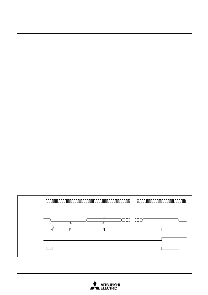
Receive
Receive is enabled when bit 2 (REi flag) of UARTi Transmit/Receive
control register 1 is set to “1.” As shown in Figure 67, the frequency
divider circuit (1/16) at the receiving side begin to work when a start
bit arrives and the data is received.
If RTSi output is selected by setting bit 2 of UARTi Transmit/Receive
control register 0 to “1”, the RTSi output is “H” when the REi flag is
“0”. When the REi flag changes to “1”, the RTSi output goes “L” to
indicate receive ready and returns to “H” once receive has started. In
other words, RTSi output can be used to determine externally
whether the receive register is ready to receive.
The entire transmission data bits are received when the start bit
passes the final bit of the receive block shown in Figure 56. At this
point, the contents of the receive register is transferred to the receive
buffer register and bit 3 (Rli flag) of UARTi Transmit/Receive control
register 1 is set to “1.” In other words, the RIi flag indicates that the
receive buffer register contains data when it is set to “1.” If RTSi out-
put is selected, RTSi output goes “L” to indicate that the register is
ready to receive the next data.
The interrupt request bit of the UARTi receive interrupt control regis-
ter is set to “1” when the RIi flag changes from “0” to “1”.
Bit 4 (OERi flag) of UARTi Transmit/Receive control register 1 is set
to “1” when the next data is transferred from the receive register to
the receive buffer register while the RIi flag is “1”, in other words,
when an overrun error occurs. If the OERi flag is “1”,
it indicates that the next data has been transferred to the receive
buffer register before the contents of the receive buffer register has
been read.
Bit 5 (FERi flag) is set to “1” when the number of stop bits is less than
required (framing error).
Bit 6 (PERi flag) is set to “1” when a parity error occurs.
Bit 7 (SUMi flag) is set to “1” when either the OERi flag, FERi flag, or
the PERi flag is set to “1.” Therefore, the SUMi flag can be used to
determine whether there is an error.
The setting of the RIi flag, OERi flag, FERi flag, and the PERi flag is
performed while transferring the contents of the receive register to
the receive buffer register. The Rli, FERi, and PERi flags are cleared
Fig. 67 Receive timing example when 8-bit asynchronous communication with no parity and 1 stop bit selected
Start bit
Stop bit
Start bit
D
0
D
1
D
7
Check to be “L” level
Starting at the falling
edge of start bit
Data fetched
Pf
i
or f
EXT
RE
i
R
X
D
i
Receive
Clock
RI
i
RTS
i
相關(guān)PDF資料 |
PDF描述 |
|---|---|
| M37754 | SINGLE-CHIP 16BIT CMOS MICROCOMPUTER |
| M37754M8C | Single Chip 16 Bits CMOS Microcomputer(16位單片機) |
| M37902F8CHP | DIODE SCHOTTKY DUAL COMMON-ANODE 25V 200mW 0.32V-vf 200mA-IFM 1mA-IF 2uA-IR SOT-23 3K/REEL |
| M37902FGCGP | SINGLE-CHIP 16-BIT CMOS MICROCOMPUTER |
| M37902FCCHP | SINGLE-CHIP 16-BIT CMOS MICROCOMPUTER |
相關(guān)代理商/技術(shù)參數(shù) |
參數(shù)描述 |
|---|---|
| M3775PR-H400CL | 制造商:Bonitron 功能描述:OVERVOLTAGE BRAKING RESISTOR |
| M3775RK-0.75A | 制造商:Bonitron 功能描述:OVERVOLTAGE BRAKING RESISTOR |
| M3775RK-C0.50A | 制造商:Bonitron 功能描述:OVERVOLTAGE BRAKING RESISTOR |
| M3775RK-C0.50B | 制造商:Bonitron 功能描述:OVERVOLTAGE BRAKING RESISTOR |
| M3775RK-C0.50C | 制造商:Bonitron 功能描述:OVERVOLTAGE BRAKING RESISTOR |
發(fā)布緊急采購,3分鐘左右您將得到回復(fù)。