- 您現(xiàn)在的位置:買賣IC網(wǎng) > PDF目錄360742 > ICS1531 Triple 8-bit MSPS A/D Converters with Line-Locked Clock Generator PDF資料下載
參數(shù)資料
| 型號: | ICS1531 |
| 英文描述: | Triple 8-bit MSPS A/D Converters with Line-Locked Clock Generator |
| 中文描述: | 三8位MSPS的的A / D轉換器與電源同步時鐘發(fā)生器 |
| 文件頁數(shù): | 62/76頁 |
| 文件大小: | 529K |
| 代理商: | ICS1531 |
第1頁第2頁第3頁第4頁第5頁第6頁第7頁第8頁第9頁第10頁第11頁第12頁第13頁第14頁第15頁第16頁第17頁第18頁第19頁第20頁第21頁第22頁第23頁第24頁第25頁第26頁第27頁第28頁第29頁第30頁第31頁第32頁第33頁第34頁第35頁第36頁第37頁第38頁第39頁第40頁第41頁第42頁第43頁第44頁第45頁第46頁第47頁第48頁第49頁第50頁第51頁第52頁第53頁第54頁第55頁第56頁第57頁第58頁第59頁第60頁第61頁當前第62頁第63頁第64頁第65頁第66頁第67頁第68頁第69頁第70頁第71頁第72頁第73頁第74頁第75頁第76頁
ICS1531 Rev N 12/1/99
December, 1999
62
Chapter 9
AC/DC Operating Conditions
ICS1531 Data Sheet - Preliminary
Copyright 1999, Integrated Circuit Systems, Inc.
All rights reserved.
9.4
AC Operating Characteristics
9.5
DC Operating Characteristics
This section lists the DC operating characteristics for the ICS1531.
9.5.1
DC Operating Characteristics for Supply Current.
Note:
All VDD measurements are taken with respect to VSS (which equals 0 V).
9.5.2
DC Operating Characteristics for Digital Inputs
Table 9-6
lists DC operating characteristics for the following ICS1531 TTL input pins:
HSYNC
PDEN
SBADR
SCL
SDA (Input mode only. For output mode, see
Table 9-7
.)
Note:
All VDD measurements are taken with respect to the VSS pin (which equals 0 V).
Note 1. Typically guaranteed by design.
9.5.3
DC Operating Characteristics for SDA Digital Pin, in Output Mode
Table 9-7
lists DC characteristics for the SDA pin output mode. (For input mode, see
Table 9-6
.)
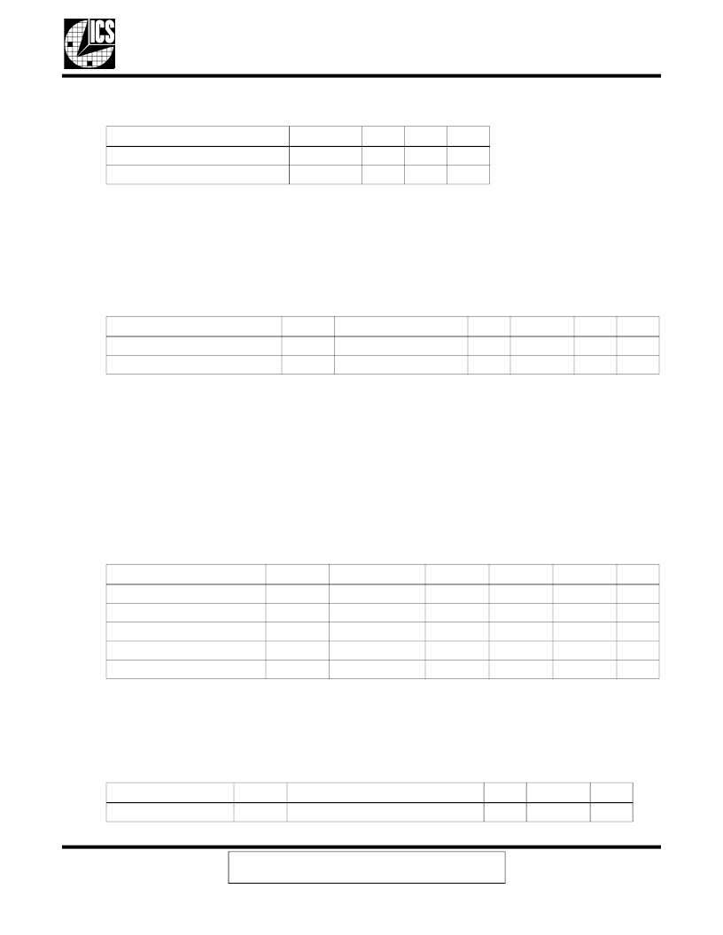
Table 9-4.
AC Operating Characteristics for ICS1531 Inputs
Parameter
Symbol
Min.
Max.
Units
Input
HSYNC: Input Frequency
f
HSYNC
f
PDEN
12
120
kHz
PDEN: Input Frequency
30
120
Hz
Table 9-5.
DC Operating Characteristics for Supply Current to ICS1531
Parameter
Symbol
Conditions
Min.
Typ.
Max.
Units
Supply Current, Digital
IDDD
VDDD = 3.3 V, 100 MHz
–
135
150
mA
Supply Current, Analog
IDDA
VDDA = 3.3 V, 100 MHz
–
125
135
mA
Table 9-6.
DC Operating Characteristics for TTL Inputs
Parameter
Symbol
Conditions
Min.
Typ.
Max.
Units
Input High Voltage
V
IH
V
IL
I
IH
I
IL
C
in
–
2.4
–
–
V
Input Low Voltage
–
–
–
0.8
V
Input High Current
V
IH
= VDD
V
IL
= 0
–
–
–
±10
μ
A
μ
A
Input Low Current
±10
–
–
Input Capacitance (Note 1)
–
10
–
pF
Table 9-7.
DC Operating Characteristics for ICS1531 SDA Pin, Output Mode
Parameter
Symbol
Conditions
Min.
Max.
Units
Output Low Voltage
V
OL
I
OUT
= 3 mA
–
0.4
V
相關PDF資料 |
PDF描述 |
|---|---|
| ICS1560M-001 | Video/Graphics Clock Generator |
| ICS1560M-003 | Video/Graphics Clock Generator |
| ICS1560N-001 | Video/Graphics Clock Generator |
| ICS1560N-003 | Video/Graphics Clock Generator |
| ICS1561AM-706 | Video/Graphics Clock Generator |
相關代理商/技術參數(shù) |
參數(shù)描述 |
|---|---|
| ICS1532 | 制造商:IDT 制造商全稱:Integrated Device Technology 功能描述:110 MHZ TRIPLE 8-BIT ADC WITH CLOCK GENERATOR |
| ICS1560M-001 | 制造商:未知廠家 制造商全稱:未知廠家 功能描述:Video/Graphics Clock Generator |
| ICS1560M-003 | 制造商:未知廠家 制造商全稱:未知廠家 功能描述:Video/Graphics Clock Generator |
| ICS1560N-001 | 制造商:未知廠家 制造商全稱:未知廠家 功能描述:Video/Graphics Clock Generator |
| ICS1560N-003 | 制造商:未知廠家 制造商全稱:未知廠家 功能描述:Video/Graphics Clock Generator |
發(fā)布緊急采購,3分鐘左右您將得到回復。