- 您現在的位置:買賣IC網 > PDF目錄370584 > HIP8112A (Harris Corporation) NTSC/PAL Video Decoder PDF資料下載
參數資料
| 型號: | HIP8112A |
| 廠商: | Harris Corporation |
| 英文描述: | NTSC/PAL Video Decoder |
| 中文描述: | NTSC / PAL視頻解碼器 |
| 文件頁數: | 24/40頁 |
| 文件大小: | 719K |
| 代理商: | HIP8112A |
第1頁第2頁第3頁第4頁第5頁第6頁第7頁第8頁第9頁第10頁第11頁第12頁第13頁第14頁第15頁第16頁第17頁第18頁第19頁第20頁第21頁第22頁第23頁當前第24頁第25頁第26頁第27頁第28頁第29頁第30頁第31頁第32頁第33頁第34頁第35頁第36頁第37頁第38頁第39頁第40頁
4-24
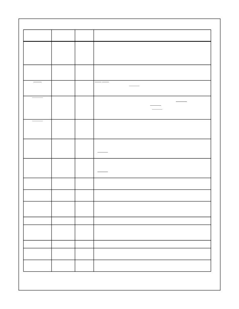
CbCr[0:7]
42, 43, 45,
47-51
Output
CbCr Data Output Port. The chrominance data output port of the decoder. Data is in
unsigned format and can range from 0 to 255. The CbCr data is subsampled to 4:2:2
format. In 4:2:2 format the CbCr bus toggles between Cb and Cr samples with the
first sample of a line always being Cb. The port is designed to minimize external logic
needed to interface to a VRAM Serial Access Port, DRAM or FIFO.
Y[0:7]
54-58, 60, 63,
64
Output
Y Data Output Port. The luminance data output port of the decoder. Data is in un-
signed format and can range from 16 to 255. The port is designed to minimize exter-
nal logic needed to interface to a VRAM Serial Access Port, DRAM or FIFO.
DVLD
66
Output
Data Valid. This pin signals when valid data is available on the data output ports. This
pin is three-stated after a RESET or software reset and should be pulled high through
a 10K resistor.
HSYNC
71
Output
Horizontal Sync. This video synchronous pulse is generated by the detection of hor-
izontal sync on the video input. In the absence of video, the HSYNC rate is set when
the internal PLL counters overflow. The HSYNC START and END time can be pro-
grammed. This pin is three-stated after a RESET or software reset and should be
pulled high through a 10K resistor.
VSYNC
70
Output
Vertical Sync. This video synchronous pulse is generated by the detection of a vertical
sync on the video input. In the absence of video the VSYNC rate is set by the over flow
of the internal line rate counter. This pin is three-stated after a RESET or software reset
and should be pulled high through a 10K resistor.
FIELD
67
Output
Field Flag. When set (‘0’) this signals that an ODD field is presently being output from
the decoder. When cleared (‘1’) this signals an EVEN field. This flag will toggle when
no vertical sync is detected and 337 lines have elapsed. This pin is three-stated after
a RESET or software reset and should be pulled high through a 10K resistor.
ACTIVE
65
Output
Active Video Flag. This flag is asserted (‘1’) when the active portion of the video line
is available on the output port. This signal is always set during Burst Output data
mode. This flag is free running and synchronous to CLK. This pin is three-stated after
a RESET or software reset and should be pulled high through a 10K resistor.
TEST
36
Input
Test input. This pin is used for production test and should be connected to digital
ground.
V
CC
26, 31, 37, 52,
59, 68, 75, 79
Input
5V Logic Supply Pins
GND
25, 33, 35, 39,
46, 53, 62, 69,
72, 80
Input
Digital Ground Pins
V
AA
2, 12,14
Input
5V Analog Supply Pins
AGND
1, 3, 10, 11,
15,16, 21, 22,
23, 24
Input
Analog GND
A/D TEST
17
Output
Chrominance ADC Test Pin. This pin should be left open.
NC
44, 61
NA
Pins used as logic outputs on later decoders. Refer to HMP8115 data sheet for de-
tails.
NC
4, 18, 20, 32,
73, 74
NA
No Connect. These pins should be left open.
Pin Description
(Continued)
NAME
PQFP PIN
NUMBER
INPUT/
OUTPUT
DESCRIPTION
HMP8112A
相關PDF資料 |
PDF描述 |
|---|---|
| HIR19-21C | Technical Data Sheet 0.8mm Height Flat Top Infrared LED |
| HIR19-L11 | Technical Data Sheet 0.8mm Height Flat Top Infrared LED |
| HIR204C | 3mm Infrared LED, T-1 |
| HIR | 5mm Infrared LED, T-1 3/4 |
| HIR333 | 5mm Infrared LED, T-1 3/4 |
相關代理商/技術參數 |
參數描述 |
|---|---|
| HIP-8V | 制造商:Belden Inc 功能描述:SPLITTER 8 WAY |
| HIP9010 | 制造商:INTERSIL 制造商全稱:Intersil Corporation 功能描述:Engine Knock Signal Processor |
| HIP9010AB | 制造商:Intersil Corporation 功能描述: |
| HIP9011 | 制造商:INTERSIL 制造商全稱:Intersil Corporation 功能描述:Engine Knock Signal Processor |
| HIP9011_06 | 制造商:INTERSIL 制造商全稱:Intersil Corporation 功能描述:Engine Knock Signal Processor |
發(fā)布緊急采購,3分鐘左右您將得到回復。