- 您現(xiàn)在的位置:買賣IC網(wǎng) > PDF目錄370584 > HIP8112A (Harris Corporation) NTSC/PAL Video Decoder PDF資料下載
參數(shù)資料
| 型號(hào): | HIP8112A |
| 廠商: | Harris Corporation |
| 英文描述: | NTSC/PAL Video Decoder |
| 中文描述: | NTSC / PAL視頻解碼器 |
| 文件頁數(shù): | 13/40頁 |
| 文件大?。?/td> | 719K |
| 代理商: | HIP8112A |
第1頁第2頁第3頁第4頁第5頁第6頁第7頁第8頁第9頁第10頁第11頁第12頁當(dāng)前第13頁第14頁第15頁第16頁第17頁第18頁第19頁第20頁第21頁第22頁第23頁第24頁第25頁第26頁第27頁第28頁第29頁第30頁第31頁第32頁第33頁第34頁第35頁第36頁第37頁第38頁第39頁第40頁
4-13
I
2
C Control Interface
The HMP8112A utilizes an I
2
C control bus interface to pro-
gram the internal configuration registers. This standard
mode (up to 100 KBPS) interface consists of the bidirectional
Serial Data Line (SDA) and the Serial Clock Line (SCL). The
implementation on the HMP8112A is a simple slave interface
that will not respond to general calls and cannot initiate a
transfer. The SDA and SCL control pins should be pulled
high through external 4k
pullup resistors to
V
CC
.
The I
2
C clock/data timing is shown below in Figure 16. The
HMP8112A always uses chip address 0x88. There are 28
internal registers used to program and configure the
decoder. The I
2
C control port contains a pointer register that
auto-increments through the entire register space and can
be written. The autoincrement pointer will wrap after the last
register has been accessed (Product ID Register) and
should be set to the desired starting address each time an
access is started. For a write transfer, the I
2
C device base
address is the first part of a serial transfer. Then the internal
register pointer is loaded and a series of registers can be
written. If multiple registers are written, the pointer register
will autoincrement up through the register address space. A
stop cycle is used to end the transfer after the desired num-
ber of registers are programmed.
For a read transfer, the I
2
C device address is the first part of
the serial transfer. Then the internal register pointer is
loaded. At this point another start cycle is initiated to access
the individual registers. Figure 18 shows the programming
flow for read transfer of the internal registers. Multiple regis-
ters can be read and the pointer register will autoincrement
up through the pointer register address space. On the last
data read, an acknowledge should not be issued. A stop
cycle is used to end the transfer after the desired number of
registers are read.
The HMP8112A contains a product ID register that can be
used to identify the presence of a board during a Plug ’n Play
detection software algorithm. The Product ID Code register is
at sub address 0x1B and always returns a data value of 0x12.
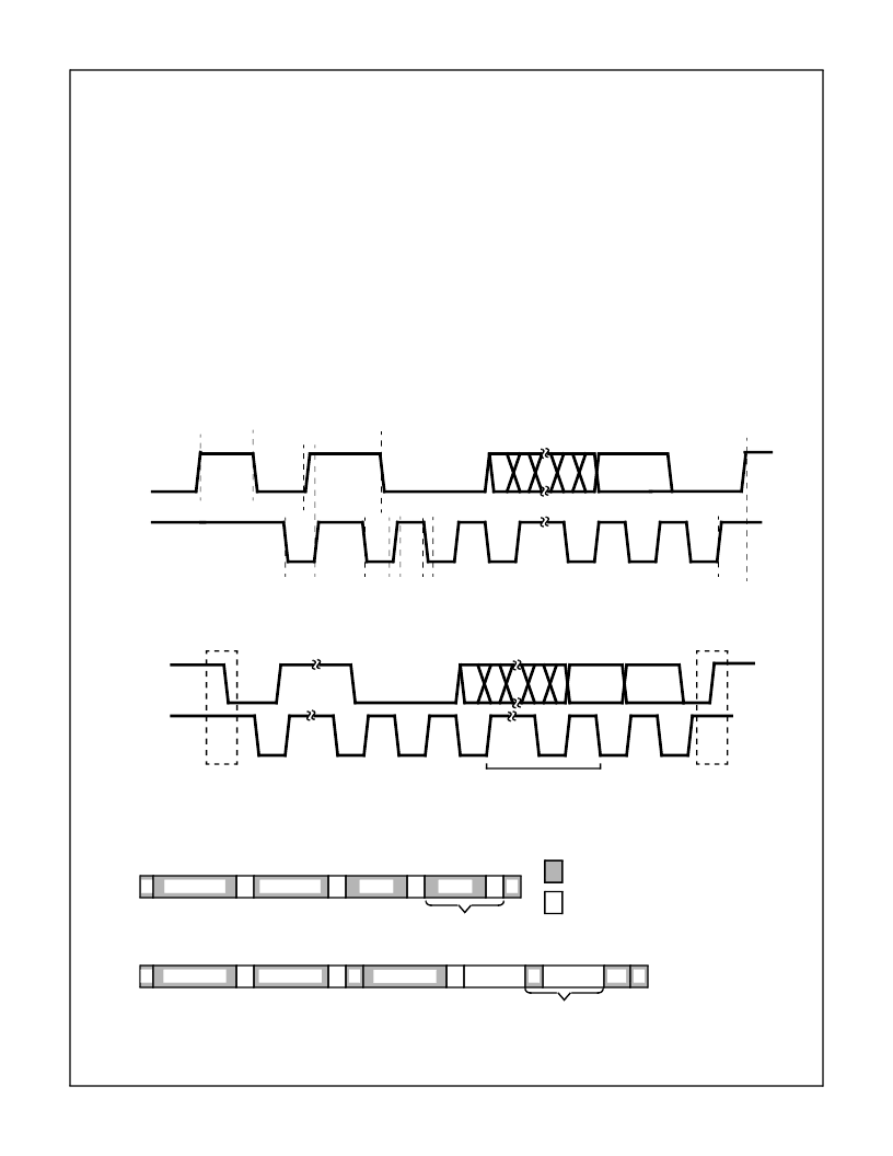
FIGURE 16. I
2
C TIMING DIAGRAM
SDA
SCL
t
BUF
t
LOW
t
HIGH
t
R
t
F
t
SU:DATA
t
HD:DATA
t
SU:STOP
SDA
SCL
START
CONDITION
S
1-7
ADDRESS
8
R/W
9
ACK
1-7
DATA
8
9
ACK
STOP
CONDITION
P
FIGURE 17. I
2
C SERIAL DATA FLOW
S = START CYCLE
P = STOP CYCLE
A = ACKNOWLEDGE
NA = NO ACKNOWLEDGE
FROM MASTER
FROM HMP8112A
0x88
DATA WRITE
DATA
DATA
0x88
DATA READ
0x89
1000 1000 (R/W)
1000 1000
FIGURE 18. REGISTER WRITE/READ FLOW
S
CHIP ADDR
A
SUB ADDR
DATA
DATA
P
NA
CHIP ADDR
S
SUB ADDR
CHIP ADDR
S
P
A
A
A
A
A
A
REGISTER
POINTED
TO BY
SUB ADDR
OPTIONAL FRAME
MAY BE REPEATED
n TIMES
A
REGISTER
POINTED
TO BY
SUB ADDR
OPTIONAL FRAME
MAY BE REPEATED
n TIMES
HMP8112A
相關(guān)PDF資料 |
PDF描述 |
|---|---|
| HIR19-21C | Technical Data Sheet 0.8mm Height Flat Top Infrared LED |
| HIR19-L11 | Technical Data Sheet 0.8mm Height Flat Top Infrared LED |
| HIR204C | 3mm Infrared LED, T-1 |
| HIR | 5mm Infrared LED, T-1 3/4 |
| HIR333 | 5mm Infrared LED, T-1 3/4 |
相關(guān)代理商/技術(shù)參數(shù) |
參數(shù)描述 |
|---|---|
| HIP-8V | 制造商:Belden Inc 功能描述:SPLITTER 8 WAY |
| HIP9010 | 制造商:INTERSIL 制造商全稱:Intersil Corporation 功能描述:Engine Knock Signal Processor |
| HIP9010AB | 制造商:Intersil Corporation 功能描述: |
| HIP9011 | 制造商:INTERSIL 制造商全稱:Intersil Corporation 功能描述:Engine Knock Signal Processor |
| HIP9011_06 | 制造商:INTERSIL 制造商全稱:Intersil Corporation 功能描述:Engine Knock Signal Processor |
發(fā)布緊急采購,3分鐘左右您將得到回復(fù)。