- 您現(xiàn)在的位置:買賣IC網(wǎng) > PDF目錄166397 > B900J24FXX12IT 0-BIT, 59.88 MHz, OTHER DSP, PQFP44 PDF資料下載
參數(shù)資料
| 型號(hào): | B900J24FXX12IT |
| 元件分類: | 數(shù)字信號(hào)處理 |
| 英文描述: | 0-BIT, 59.88 MHz, OTHER DSP, PQFP44 |
| 文件頁數(shù): | 36/100頁 |
| 文件大?。?/td> | 1547K |
| 代理商: | B900J24FXX12IT |
第1頁第2頁第3頁第4頁第5頁第6頁第7頁第8頁第9頁第10頁第11頁第12頁第13頁第14頁第15頁第16頁第17頁第18頁第19頁第20頁第21頁第22頁第23頁第24頁第25頁第26頁第27頁第28頁第29頁第30頁第31頁第32頁第33頁第34頁第35頁當(dāng)前第36頁第37頁第38頁第39頁第40頁第41頁第42頁第43頁第44頁第45頁第46頁第47頁第48頁第49頁第50頁第51頁第52頁第53頁第54頁第55頁第56頁第57頁第58頁第59頁第60頁第61頁第62頁第63頁第64頁第65頁第66頁第67頁第68頁第69頁第70頁第71頁第72頁第73頁第74頁第75頁第76頁第77頁第78頁第79頁第80頁第81頁第82頁第83頁第84頁第85頁第86頁第87頁第88頁第89頁第90頁第91頁第92頁第93頁第94頁第95頁第96頁第97頁第98頁第99頁第100頁
B900
Advance Data Sheet
Baseband Signal Processor
July 1999
40
Lucent Technologies Inc.
5 Software Architecture (continued)
5.1
Instruction Set (continued)
5.1.1 F1 Multiply/ALU Instructions (continued)
Note: For transfer statements when loading the upper half of an accumulator, the lower half is cleared if the
corresponding CLR bit in the auc register is zero. auc is cleared by reset.
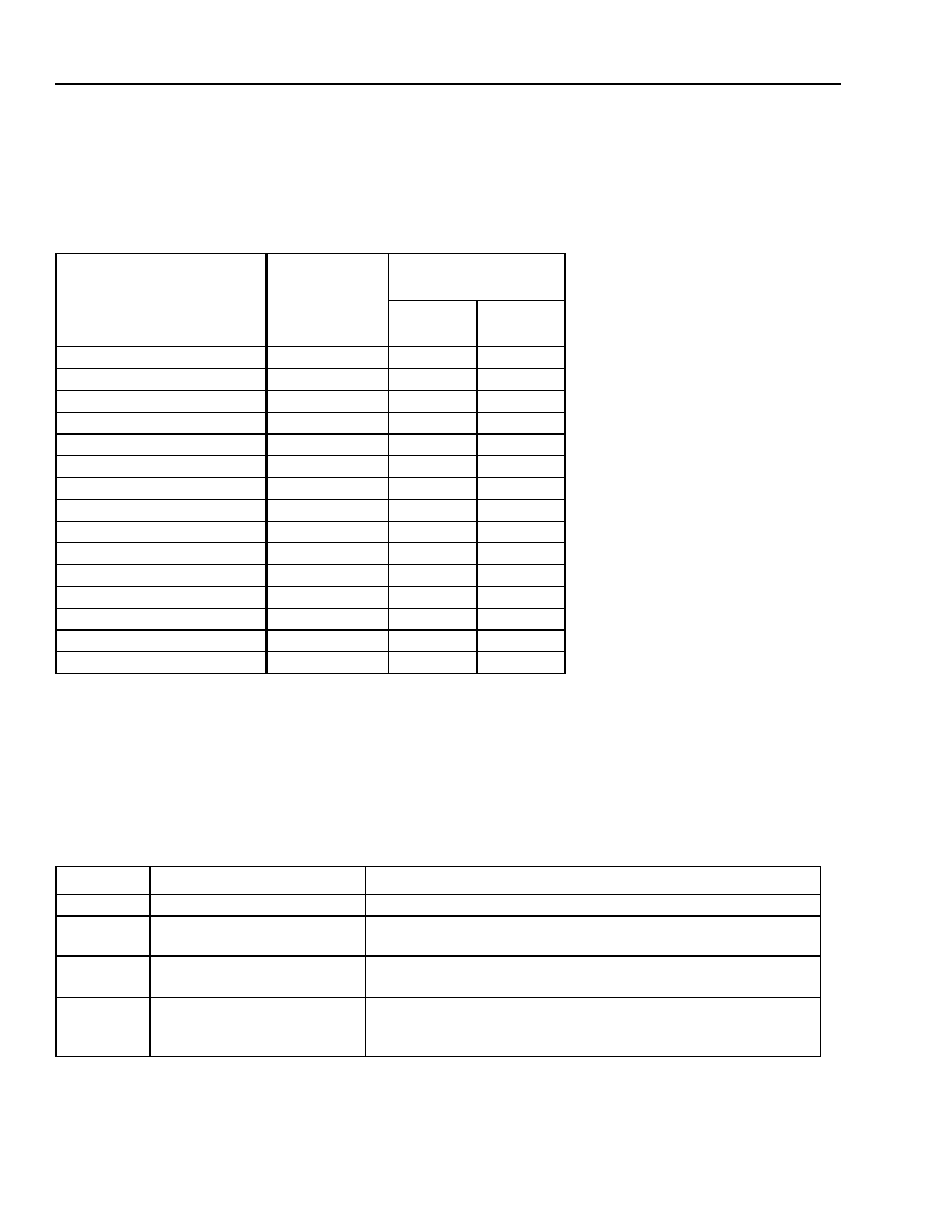
Table 22. F1 Multiply/ALU Instructions
F1 Function Statement
Transfer
Statement*
* The [l] is an optional argument that specifies the low 16 bits of aT or y.
Transfer Statement
Cycles
If an X space access and a Y space access are made to the same bank of DPRAM in one
instruction, add one cycle.
Not Using
Cache
Using
Cache
p = x
y
p = x
y becomes a single-cycle squaring operation if the auc bit 7 is set. With bit 7 set, a
transfer statement of the form y = Y loads the x register and the y register with the same
number, so p = x
y results in the square.
y = Y, x = X
2
1
aD = p, p = x
y = aT, x = X
2
1
aD = aS + p, p = x
y[l] = Y
1
aD = aS – p, p = x
aT[l] = Y
1
aD = p
x = Y
1
aD = aS + p
Y
1
aD = aS – p
Y = y[l]
2
aD = y
Y = aT[l]
2
aD = aS + y
Z:y, x = X
2
aD = aS – y
Z:y[l]
2
aD = aS & y
Z:aT[l]
2
aD = aS | y
—
1
aD = aS ^ y
—
1
aS – y
—
1
aS & y
—
1
Table 23. Replacement Table for F1 Multiply/ALU Instructions
Replace
Value
Meaning
aD, aS, aT
a0, a1
One of the DAU accumulators.
X
*pt++, *pt++i
X space memory location pointed to by pt.
pt is postmodified by +1 and i, respectively.
Y
*rM, *rM++, *rM– –, *rM++j
RAM location pointed to by rM (M = 0, 1, 2, 3).
rM is postmodified by 0, +1, –1, or j, respectively.
Z
*rMzp, *rMpz, *rMm2, *rMjk
Read/write compound addressing. rM (M = 0, 1, 2, 3) is used
twice. First, postmodified by 0, +1, –1, or j, respectively; and,
second, postmodified by +1, 0, +2, or k, respectively.
相關(guān)PDF資料 |
PDF描述 |
|---|---|
| BA00CC0WCP-V5 | 1A Low Dropout Voltage Regulator with Shut Down Switch(Adustable Voltage) |
| BA10E6 | COPPER ALLOY, TIN FINISH, RING TERMINAL |
| BA12004 | 0.5 A, 7 CHANNEL, NPN, Si, POWER TRANSISTOR |
| BA1518SUR5VP | SINGLE COLOR DISPLAY CLUSTER, ULTRA RED |
| BA1524LUR5VP | SINGLE COLOR DISPLAY CLUSTER, ULTRA RED |
相關(guān)代理商/技術(shù)參數(shù) |
參數(shù)描述 |
|---|---|
| B-900-M-10 | 制造商:Thomas & Betts 功能描述: |
| B-900-M-10-EG | 制造商:Thomas & Betts 功能描述: |
| B-900-M-20 | 制造商:Thomas & Betts 功能描述: |
| B-900-M-20-EG | 制造商:Thomas & Betts 功能描述: |
| B901 | 制造商:EDAL 制造商全稱:EDAL 功能描述:Silicon Bridge Rectifier |
發(fā)布緊急采購,3分鐘左右您將得到回復(fù)。