- 您現(xiàn)在的位置:買賣IC網(wǎng) > PDF目錄374046 > ADV7162KS220 (ANALOG DEVICES INC) 96-Bit, 220 MHz True-Color Video RAM-DAC PDF資料下載
參數(shù)資料
| 型號(hào): | ADV7162KS220 |
| 廠商: | ANALOG DEVICES INC |
| 元件分類: | 顯示控制器 |
| 英文描述: | 96-Bit, 220 MHz True-Color Video RAM-DAC |
| 中文描述: | 1600 X 1200 PIXELS PALETTE-DAC DSPL CTLR, PQFP160 |
| 封裝: | PLASTIC, QFP-160 |
| 文件頁(yè)數(shù): | 17/44頁(yè) |
| 文件大小: | 668K |
| 代理商: | ADV7162KS220 |
第1頁(yè)第2頁(yè)第3頁(yè)第4頁(yè)第5頁(yè)第6頁(yè)第7頁(yè)第8頁(yè)第9頁(yè)第10頁(yè)第11頁(yè)第12頁(yè)第13頁(yè)第14頁(yè)第15頁(yè)第16頁(yè)當(dāng)前第17頁(yè)第18頁(yè)第19頁(yè)第20頁(yè)第21頁(yè)第22頁(yè)第23頁(yè)第24頁(yè)第25頁(yè)第26頁(yè)第27頁(yè)第28頁(yè)第29頁(yè)第30頁(yè)第31頁(yè)第32頁(yè)第33頁(yè)第34頁(yè)第35頁(yè)第36頁(yè)第37頁(yè)第38頁(yè)第39頁(yè)第40頁(yè)第41頁(yè)第42頁(yè)第43頁(yè)第44頁(yè)
ADV7160/ADV7162
REV. 0
–17–
ADV7160/
ADV7162
LOADOUT
LOADIN
BLANK
SCKOUT
SCKIN
LATCH
EN
CLOCK
CLOCK
TO
TTL
DIVIDE BY
M (
÷
M)
DIVIDE BY
N (
÷
N)
PRGCKOUT
S
E
L
E
C
T
PLLREF
TO COLOR DATA
MULTIPLEXER
TRISYNC
PLL
SYNC
M IS A FUNCTION OF MULTIPLEX RATE
M = 8 IN 8:1 MULTIPLEX MODE
M = 4 IN 4:1 MULTIPLEX MODE
M = 2 IN 2:1 MULTIPLEX MODE
N IS INDEPENDENTLY PROGRAMMABLE
N = (4, 8, 16, 32)
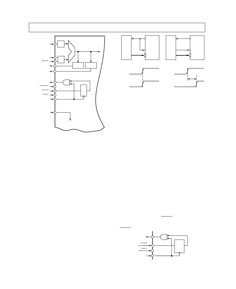
Figure 16. Clock Control Circuit of the ADV7160/ADV7162
CLOCK CONTROL SIGNALS
LOADOUT
The ADV7160/ADV7162 generates a LOADOUT control sig-
nal which runs at a divided down frequency of the pixel
CLOCK. The frequency is automatically set to the pro-
grammed multiplex rate, controlled by CR37 and CR36 of
Command Register 3.
f
LOADOUT
= f
CLOCK
/8
f
LOADOUT
= f
CLOCK
/4
f
LOADOUT
= f
CLOCK
/2
The LOADOUT signal is used to directly drive the LOADIN
pixel latch signal of the ADV7160/ADV7162. This is most sim-
ply achieved by tying the LOADOUT and LOADIN pins to-
gether. Alternatively, the LOADOUT signal can be used to
drive the frame buffer’s shift clock signals, returning to the
LOADIN input delayed with respect to LOADOUT.
If it is not necessary to have a known fixed number of pipeline
delays, then there is no limitation on the delay between
LOADOUT and LOADIN (LOADOUT(1) and
LOADOUT(2)). LOADIN and Pixel Data must conform to
the setup and hold times (t
8
and t
9
).
If however, it is required that the ADV7160/ADV7162 has
a fixed number of pipeline delays (t
PD
) LOADOUT and
LOADIN must conform to timing specifications t
10
and
τ
–t
11
as
illustrated in Figures 5 to 10.
8:1 multiplex mode
4:1 multiplex mode
2:1 multiplex mode
ADV7160/
ADV7162
LOADOUT
LOADIN
PIXEL
DATA
VIDEO
FRAME
BUFFER
LOADOUT(1)
LOADOUT(2)
ADV7160/
ADV7162
LOADOUT
LOADIN
PIXEL
DATA
VIDEO
FRAME
BUFFER
LOADOUT
LOADIN
LOADOUT(1)
LOADOUT(2)
DELAY
Figure 17. LOADOOUT vs Pixel Clock
Pipeline Delay and Onboard Calibration
The ADV7160/ADV7162 has a fixed number of pipeline delays
(t
PD
), so long as timings t
10
and
τ
–t
11
are met. However, if a
fixed number of pipeline delays is not a requirement, timings t
10
and
τ
–t
11
can be ignored, a calibration cycle must be run and
there is no restriction on LOADIN to LOADOUT timing. If
timings t
10
and
τ
–t
11
are not met, the part will function correctly
though with an increased number of pipeline delays. The
ADV7160/ADV7162 has on-board calibration circuitry which
synchronizes pixel data and LOADIN with the internal
ADV7160/ADV7162 clocking signals. Calibration can be per-
formed in two ways. During the device’s initialization sequence
by toggling two bits of the Mode Register, MR10 followed by
MR15 or by writing a “1” to Bit CR10 of Command Register 1
and a “0” to MR15 which executes a calibration on every
Vertical Sync.
PRGCKOUT
The PRGCKOUT control signal outputs a user programmable
clock frequency. It is a divided down frequency of the pixel
CLOCK (see Figure 11). The rising edge of PRGCKOUT is
synchronous to the rising edge of LOADOUT.
f
PRGCKOUT
=
f
CLOCK
/N
where
N
= 4, 8, 16 or 32.
One application of the PRGCKOUT is to use it as the master
clock frequency of the graphics subsystems processor or
controller.
SCKIN, SCKOUT
These video memory signals are used to minimize external sup-
port chips. Figure 18 illustrates the function that is provided.
An input signal applied to SCKIN is synchronously AND-ed
with the video blanking signal (
BLANK
). The resulting signal
is output on SCKOUT. Figure 12 of the Timing Waveform
section shows the relationship between SCKOUT, SCKIN and
BLANK
.
BLANK
SCKOUT
SCKIN
LATCH
ENABLE
SYNC
Figure 18. SCKOUT Generation Circuit
相關(guān)PDF資料 |
PDF描述 |
|---|---|
| ADV7160KS140 | 96-Bit, 220 MHz True-Color Video RAM-DAC |
| ADV7160KS170 | 96-Bit, 220 MHz True-Color Video RAM-DAC |
| ADV7160KS220 | 96-Bit, 220 MHz True-Color Video RAM-DAC |
| ADV7170 | Digital PAL/NTSC Video Encoder with 10-Bit SSAF⑩ and Advanced Power Management |
| ADV7170KS | Digital PAL/NTSC Video Encoder with 10-Bit SSAF⑩ and Advanced Power Management |
相關(guān)代理商/技術(shù)參數(shù) |
參數(shù)描述 |
|---|---|
| ADV7162KSZ140 | 制造商:Analog Devices 功能描述:DAC 3-CH Segment 10-bit 160-Pin MQFP |
| ADV7162KSZ220 | 制造商:Analog Devices 功能描述:DAC 3-CH Segment 10-bit 160-Pin MQFP |
| ADV7170 | 制造商:AD 制造商全稱:Analog Devices 功能描述:Digital PAL/NTSC Video Encoder with 10-Bit SSAF⑩ and Advanced Power Management |
| ADV71707911 | 制造商:LG Corporation 功能描述:FRAME ASSEMBLY |
| ADV7170KS | 制造商:AD 制造商全稱:Analog Devices 功能描述:Digital PAL/NTSC Video Encoder with 10-Bit SSAF⑩ and Advanced Power Management |
發(fā)布緊急采購(gòu),3分鐘左右您將得到回復(fù)。