- 您現(xiàn)在的位置:買賣IC網(wǎng) > PDF目錄1887 > 5AGXMB3G6F31C6NES (Altera)IC ARRIA V FPGA 362K 896FBGA PDF資料下載
參數(shù)資料
| 型號: | 5AGXMB3G6F31C6NES |
| 廠商: | Altera |
| 文件頁數(shù): | 18/124頁 |
| 文件大小: | 0K |
| 描述: | IC ARRIA V FPGA 362K 896FBGA |
| 標(biāo)準(zhǔn)包裝: | 3 |
| 系列: | Arria V GX |
| LAB/CLB數(shù): | 17110 |
| 邏輯元件/單元數(shù): | 362730 |
| RAM 位總計(jì): | 2148352 |
| 輸入/輸出數(shù): | 384 |
| 電源電壓: | 1.07 V ~ 1.13 V |
| 安裝類型: | 表面貼裝 |
| 工作溫度: | 0°C ~ 85°C |
| 封裝/外殼: | 896-BGA |
| 供應(yīng)商設(shè)備封裝: | 896-FBGA(31x31) |
| 其它名稱: | 544-2735 |
第1頁第2頁第3頁第4頁第5頁第6頁第7頁第8頁第9頁第10頁第11頁第12頁第13頁第14頁第15頁第16頁第17頁當(dāng)前第18頁第19頁第20頁第21頁第22頁第23頁第24頁第25頁第26頁第27頁第28頁第29頁第30頁第31頁第32頁第33頁第34頁第35頁第36頁第37頁第38頁第39頁第40頁第41頁第42頁第43頁第44頁第45頁第46頁第47頁第48頁第49頁第50頁第51頁第52頁第53頁第54頁第55頁第56頁第57頁第58頁第59頁第60頁第61頁第62頁第63頁第64頁第65頁第66頁第67頁第68頁第69頁第70頁第71頁第72頁第73頁第74頁第75頁第76頁第77頁第78頁第79頁第80頁第81頁第82頁第83頁第84頁第85頁第86頁第87頁第88頁第89頁第90頁第91頁第92頁第93頁第94頁第95頁第96頁第97頁第98頁第99頁第100頁第101頁第102頁第103頁第104頁第105頁第106頁第107頁第108頁第109頁第110頁第111頁第112頁第113頁第114頁第115頁第116頁第117頁第118頁第119頁第120頁第121頁第122頁第123頁第124頁
Page 42
Configuration Specification
Arria V GZ Device Datasheet
February 2014
Altera Corporation
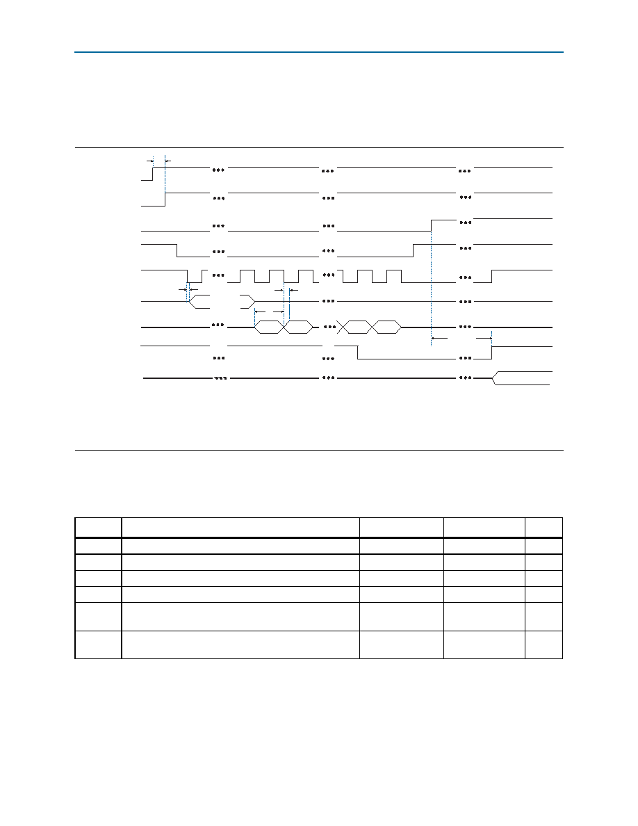
Active Serial Configuration Timing
Figure 8 shows the timing waveform for the active serial (AS) x1 mode and AS x4
mode configuration timing.
Table 47 lists the timing parameters for AS x1 and AS x4 configurations in Arria V GZ
devices.
Figure 8. AS Configuration Timing
Notes to Figure 8:
(1) If you are using AS ×4 mode, this signal represents the AS_DATA[3..0] and EPCQ sends in 4-bits of data for each DCLK cycle.
(2) The initialization clock can be from internal oscillator or CLKUSR pin.
(3) After the option bit to enable the INIT_DONE pin is configured into the device, the INIT_DONE goes low.
Read Address
bit 1
bit 0
bit (n
2) bit (n 1)
tCD2UM
nSTATUS
nCONFIG
CONF_DONE
nCSO
DCLK
AS_DATA0/ASDO
AS_DATA1 (1)
INIT_DONE (3)
User I/O
User Mode
tCF2ST1
tDH
tSU
tCO
(2)
Table 47. AS Timing Parameters for AS x1 and AS x4 Configurations in Arria V GZ Devices (1), (2)
Symbol
Parameter
Minimum
Maximum
Unit
tCO
DCLK
falling edge to AS_DATA0/ASDO output
—
4
ns
tSU
Data setup time before falling edge on DCLK
1.5
—
ns
tH
Data hold time after falling edge on DCLK
0—
ns
tCD2UM
CONF_DONE
high to user mode (3)
175
437
μs
tCD2CU
CONF_DONE
high to CLKUSR enabled
4 × maximum DCLK
period
——
tCD2UMC
CONF_DONE
high to user mode with CLKUSR option on
tCD2CU + (17,408
×
CLKUSR
period)
——
Notes to Table 47:
(1) The minimum and maximum numbers apply only if you choose the internal oscillator as the clock source for initializing the device.
(2) tCF2CD, tCF2ST0, tCFG, tSTATUS, and tCF2ST1 timing parameters are identical to the timing parameters for PS mode listed in Table 49 on page 44.
(3) To enable the CLKUSR pin as the initialization clock source and to obtain the maximum frequency specification on this pin, refer to the
“Initialization” section of the Configuration, Design Security, and Remote System Upgrades in Arria V Devices chapter.
相關(guān)PDF資料 |
PDF描述 |
|---|---|
| 5CGXFC7D7F31C8NES | IC CYCLONE V FPGA 150K 896-FBGA |
| 668-0003-C | IC CPU RABBIT2000 30MHZ 100PQFP |
| 668-0011 | IC MPU RABIT3000A 55.5MHZ128LQFP |
| 6PAIC3106IRGZRQ1 | IC AUDIO CODEC STEREO 48-QFN |
| 70001851 | DEVICE SERVER 1PORT SRL-ETHERNET |
相關(guān)代理商/技術(shù)參數(shù) |
參數(shù)描述 |
|---|---|
| 5AGXMB3G6F35C6N | 功能描述:FPGA - 現(xiàn)場可編程門陣列 FPGA - Arria V GX 13688 LABs 544 IOs RoHS:否 制造商:Altera Corporation 系列:Cyclone V E 柵極數(shù)量: 邏輯塊數(shù)量:943 內(nèi)嵌式塊RAM - EBR:1956 kbit 輸入/輸出端數(shù)量:128 最大工作頻率:800 MHz 工作電源電壓:1.1 V 最大工作溫度:+ 70 C 安裝風(fēng)格:SMD/SMT 封裝 / 箱體:FBGA-256 |
| 5AGXMB3G6F40C6N | 功能描述:FPGA - 現(xiàn)場可編程門陣列 FPGA - Arria V GX 13688 LABs 704 IOs RoHS:否 制造商:Altera Corporation 系列:Cyclone V E 柵極數(shù)量: 邏輯塊數(shù)量:943 內(nèi)嵌式塊RAM - EBR:1956 kbit 輸入/輸出端數(shù)量:128 最大工作頻率:800 MHz 工作電源電壓:1.1 V 最大工作溫度:+ 70 C 安裝風(fēng)格:SMD/SMT 封裝 / 箱體:FBGA-256 |
| 5AGXMB5G4F35C4N | 功能描述:FPGA - 現(xiàn)場可編程門陣列 FPGA - Arria V GX 15849 LABs 544 IOs RoHS:否 制造商:Altera Corporation 系列:Cyclone V E 柵極數(shù)量: 邏輯塊數(shù)量:943 內(nèi)嵌式塊RAM - EBR:1956 kbit 輸入/輸出端數(shù)量:128 最大工作頻率:800 MHz 工作電源電壓:1.1 V 最大工作溫度:+ 70 C 安裝風(fēng)格:SMD/SMT 封裝 / 箱體:FBGA-256 |
| 5AGXMB5G4F35C5G | 功能描述:1152-PIN FBGA 制造商:altera 系列:Arria V GX 零件狀態(tài):在售 LAB/CLB 數(shù):19811 邏輯元件/單元數(shù):420000 總 RAM 位數(shù):23625728 I/O 數(shù):544 電壓 - 電源:1.07 V ~ 1.13 V 工作溫度:0°C ~ 85°C(TJ) 標(biāo)準(zhǔn)包裝:24 |
| 5AGXMB5G4F35C5N | 功能描述:FPGA - 現(xiàn)場可編程門陣列 FPGA - Arria V GX 15849 LABs 544 IOs RoHS:否 制造商:Altera Corporation 系列:Cyclone V E 柵極數(shù)量: 邏輯塊數(shù)量:943 內(nèi)嵌式塊RAM - EBR:1956 kbit 輸入/輸出端數(shù)量:128 最大工作頻率:800 MHz 工作電源電壓:1.1 V 最大工作溫度:+ 70 C 安裝風(fēng)格:SMD/SMT 封裝 / 箱體:FBGA-256 |
發(fā)布緊急采購,3分鐘左右您將得到回復(fù)。