- 您現(xiàn)在的位置:買賣IC網(wǎng) > PDF目錄375005 > XCB56364PV100 (MOTOROLA INC) 24-Bit Audio Digital Signal Processor PDF資料下載
參數(shù)資料
| 型號(hào): | XCB56364PV100 |
| 廠商: | MOTOROLA INC |
| 元件分類: | 數(shù)字信號(hào)處理 |
| 英文描述: | 24-Bit Audio Digital Signal Processor |
| 中文描述: | 8-BIT, 100 MHz, OTHER DSP, PQFP112 |
| 封裝: | QFP-112 |
| 文件頁(yè)數(shù): | 22/162頁(yè) |
| 文件大?。?/td> | 2405K |
| 代理商: | XCB56364PV100 |
第1頁(yè)第2頁(yè)第3頁(yè)第4頁(yè)第5頁(yè)第6頁(yè)第7頁(yè)第8頁(yè)第9頁(yè)第10頁(yè)第11頁(yè)第12頁(yè)第13頁(yè)第14頁(yè)第15頁(yè)第16頁(yè)第17頁(yè)第18頁(yè)第19頁(yè)第20頁(yè)第21頁(yè)當(dāng)前第22頁(yè)第23頁(yè)第24頁(yè)第25頁(yè)第26頁(yè)第27頁(yè)第28頁(yè)第29頁(yè)第30頁(yè)第31頁(yè)第32頁(yè)第33頁(yè)第34頁(yè)第35頁(yè)第36頁(yè)第37頁(yè)第38頁(yè)第39頁(yè)第40頁(yè)第41頁(yè)第42頁(yè)第43頁(yè)第44頁(yè)第45頁(yè)第46頁(yè)第47頁(yè)第48頁(yè)第49頁(yè)第50頁(yè)第51頁(yè)第52頁(yè)第53頁(yè)第54頁(yè)第55頁(yè)第56頁(yè)第57頁(yè)第58頁(yè)第59頁(yè)第60頁(yè)第61頁(yè)第62頁(yè)第63頁(yè)第64頁(yè)第65頁(yè)第66頁(yè)第67頁(yè)第68頁(yè)第69頁(yè)第70頁(yè)第71頁(yè)第72頁(yè)第73頁(yè)第74頁(yè)第75頁(yè)第76頁(yè)第77頁(yè)第78頁(yè)第79頁(yè)第80頁(yè)第81頁(yè)第82頁(yè)第83頁(yè)第84頁(yè)第85頁(yè)第86頁(yè)第87頁(yè)第88頁(yè)第89頁(yè)第90頁(yè)第91頁(yè)第92頁(yè)第93頁(yè)第94頁(yè)第95頁(yè)第96頁(yè)第97頁(yè)第98頁(yè)第99頁(yè)第100頁(yè)第101頁(yè)第102頁(yè)第103頁(yè)第104頁(yè)第105頁(yè)第106頁(yè)第107頁(yè)第108頁(yè)第109頁(yè)第110頁(yè)第111頁(yè)第112頁(yè)第113頁(yè)第114頁(yè)第115頁(yè)第116頁(yè)第117頁(yè)第118頁(yè)第119頁(yè)第120頁(yè)第121頁(yè)第122頁(yè)第123頁(yè)第124頁(yè)第125頁(yè)第126頁(yè)第127頁(yè)第128頁(yè)第129頁(yè)第130頁(yè)第131頁(yè)第132頁(yè)第133頁(yè)第134頁(yè)第135頁(yè)第136頁(yè)第137頁(yè)第138頁(yè)第139頁(yè)第140頁(yè)第141頁(yè)第142頁(yè)第143頁(yè)第144頁(yè)第145頁(yè)第146頁(yè)第147頁(yè)第148頁(yè)第149頁(yè)第150頁(yè)第151頁(yè)第152頁(yè)第153頁(yè)第154頁(yè)第155頁(yè)第156頁(yè)第157頁(yè)第158頁(yè)第159頁(yè)第160頁(yè)第161頁(yè)第162頁(yè)
Specifications
Thermal Characteristics
2-2
DSP56364 Advance Information
MOTOROLA
2.3
THERMAL CHARACTERISTICS
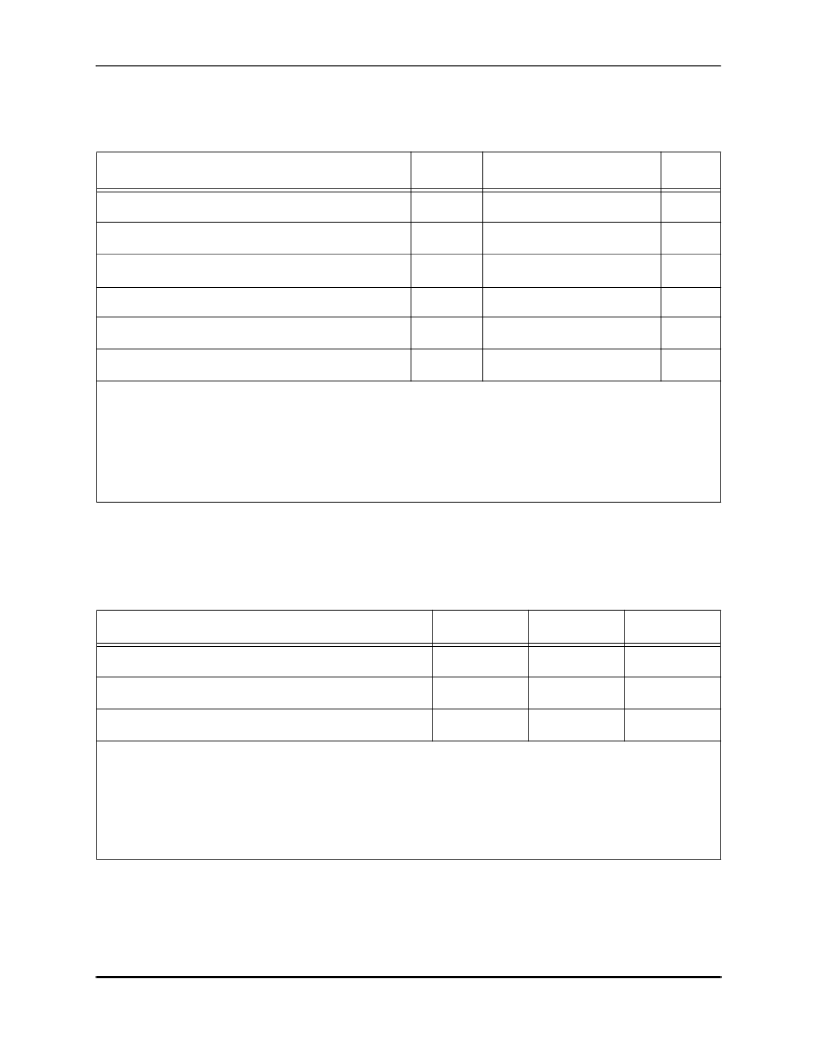
Table 2-1 Maximum Ratings
Rating
1
Symbol
Value
1, 2
Unit
Supply Voltage
V
CC
0.3 to +4.0
V
All input voltages excluding “5 V tolerant” inputs
3
V
IN
GND -0.3 to V
CC
+ 0.3
V
All “5 V tolerant” input voltages
3
V
IN5
GND
0.3 to V
CC
+ 3.95
V
Current drain per pin excluding V
CC
and GND
I
10
mA
Operating temperature range
T
J
-40 to +105
°
C
Storage temperature
T
STG
55 to +125
°
C
Notes:
1.
2.
GND = 0 V, V
CC
= 3.3 V
±
0.16 V, T
J
= –0
°
C to +105
°
C, CL = 50 pF
Absolute maximum ratings are stress ratings only, and functional operation at the maximum is not
guaranteed. Stress beyond the maximum rating may affect device reliability or cause permanent
damage to the device.
CAUTION
: All “5 V Tolerant” input voltages must not be more than 3.95 V greater than the supply
voltage; this restriction applies to “power on”, as well as during normal operation. In any case, the
input voltages cannot be more than 5.75 V. “5 V Tolerant” inputs are inputs that tolerate 5 V.
3.
Table 2-2 Thermal Characteristics
Characteristic
Symbol
TQFP Value
Unit
Junction-to-ambient thermal resistance
1
R
θ
JA
or
θ
JA
49.87
°
C/W
Junction-to-case thermal resistance
2
R
θ
JC
or
θ
JC
9.26
°
C/W
Thermal characterization parameter
Ψ
JT
2.0
°
C/W
Notes:
1.
Junction-to-ambient thermal resistance is based on measurements on a horizontal single-sided
printed circuit board per SEMI G38-87 in natural convection.(SEMI is Semiconductor Equipment and
Materials International, 805 East Middlefield Rd., Mountain View, CA 94043, (415) 964-5111.)
Measurements were done with parts mounted on thermal test boards conforming to specification
EIA/JESD51-3.
Junction-to-case thermal resistance is based on measurements using a cold plate per SEMI G30-88,
with the exception that the cold plate temperature is used for the case temperature.
2.
F
Freescale Semiconductor, Inc.
For More Information On This Product,
Go to: www.freescale.com
n
.
相關(guān)PDF資料 |
PDF描述 |
|---|---|
| XCCACE-TQ144 | System ACE CompactFlash Solution |
| XCCACE-TQ144I | System ACE CompactFlash Solution |
| XCCACE128-I | System ACE CompactFlash Solution |
| XCCACE256-I | System ACE CompactFlash Solution |
| XCCACEM16BG388I | System ACE MPM Solution |
相關(guān)代理商/技術(shù)參數(shù) |
參數(shù)描述 |
|---|---|
| XCBC01 | 制造商:Excelsys Technologies 功能描述:CONF POWER CHASSIS 700W 6 SLOT |
| XCBMV0502 A | 制造商:Lap Electrical Ltd 功能描述:10-100V 2W AMB XENON BCN |
| XCBMV0502 B | 制造商:Lap Electrical Ltd 功能描述:10-100V 2W BLU XENON BCN |
| XCBMV0502 R | 制造商:Lap Electrical Ltd 功能描述:10-100V 2W RED XENON BCN |
| XCBMV0606 A | 制造商:Lap Electrical Ltd 功能描述:10-100V 6W AMB XENON BCN |
發(fā)布緊急采購(gòu),3分鐘左右您將得到回復(fù)。