- 您現(xiàn)在的位置:買賣IC網(wǎng) > PDF目錄17007 > USB-I2C/LIN-CONV-Z (Analog Devices Inc)USB TO I2C/LIN CONV BOARD PDF資料下載
參數(shù)資料
| 型號: | USB-I2C/LIN-CONV-Z |
| 廠商: | Analog Devices Inc |
| 文件頁數(shù): | 30/104頁 |
| 文件大?。?/td> | 0K |
| 描述: | USB TO I2C/LIN CONV BOARD |
| 標準包裝: | 1 |
| 附件類型: | 適配器板 |
| 適用于相關(guān)產(chǎn)品: | ARM7TDMI? |
第1頁第2頁第3頁第4頁第5頁第6頁第7頁第8頁第9頁第10頁第11頁第12頁第13頁第14頁第15頁第16頁第17頁第18頁第19頁第20頁第21頁第22頁第23頁第24頁第25頁第26頁第27頁第28頁第29頁當前第30頁第31頁第32頁第33頁第34頁第35頁第36頁第37頁第38頁第39頁第40頁第41頁第42頁第43頁第44頁第45頁第46頁第47頁第48頁第49頁第50頁第51頁第52頁第53頁第54頁第55頁第56頁第57頁第58頁第59頁第60頁第61頁第62頁第63頁第64頁第65頁第66頁第67頁第68頁第69頁第70頁第71頁第72頁第73頁第74頁第75頁第76頁第77頁第78頁第79頁第80頁第81頁第82頁第83頁第84頁第85頁第86頁第87頁第88頁第89頁第90頁第91頁第92頁第93頁第94頁第95頁第96頁第97頁第98頁第99頁第100頁第101頁第102頁第103頁第104頁
Data Sheet
ADuC7019/20/21/22/24/25/26/27/28/29
Rev. F | Page 31 of 104
ADUC7028
A
8
7
6
5
4
3
2
1
B
C
D
E
F
G
H
BOTTOM VIEW
(Not to Scale)
04955-
086
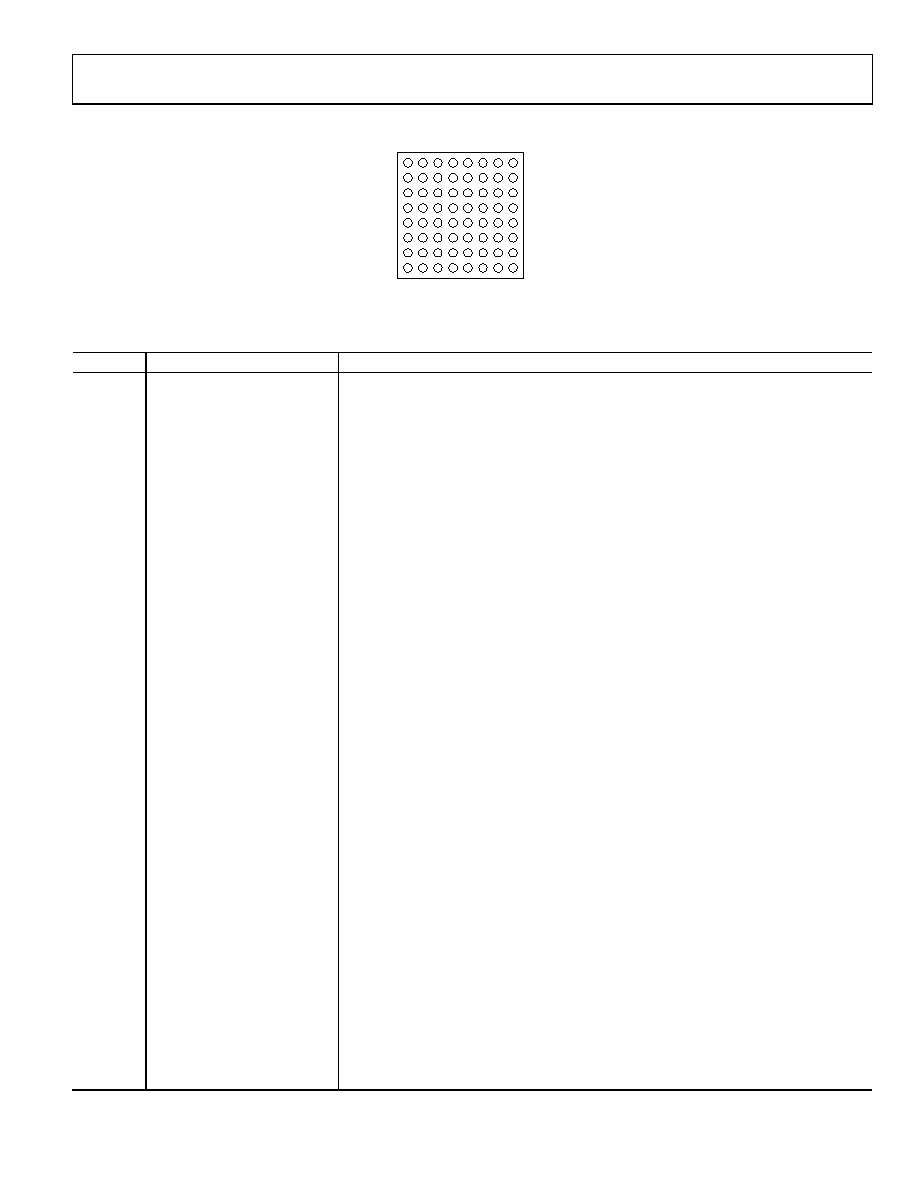
Figure 26. 64-Ball CSP_BGA Pin Configuration (ADuC7028)
Table 14. Pin Function Descriptions (ADuC7028)
Ball No.
Mnemonic
Description
A1
ADC3/CMP1
Single-Ended or Differential Analog Input 3/Comparator Negative Input.
A2
DACVDD
3.3 V Power Supply for the DACs. Must be connected to AVDD.
A3
AVDD
3.3 V Analog Power.
A4
AGND
Analog Ground. Ground reference point for the analog circuitry.
A5
DACGND
Ground for the DAC. Typically connected to AGND.
A6
P4.2/PLAO[10]
General-Purpose Input and Output Port 4.2/Programmable Logic Array Output Element 10.
A7
P1.1/SPM1/PLAI[1]
Serial Port Multiplexed. General-Purpose Input and Output Port 1.1/UART, I2C0/Programmable
Logic Array Input Element 1.
A8
P1.2/SPM2/PLAI[2]
Serial Port Multiplexed. General-Purpose Input and Output Port 1.2/UART, I2C1/Programmable
Logic Array Input Element 2.
B1
ADC4
Single-Ended or Differential Analog Input 4.
B2
ADC2/CMP0
Single-Ended or Differential Analog Input 2/Comparator Positive Input.
B3
ADC1
Single-Ended or Differential Analog Input 1.
B4
DACREF
External Voltage Reference for the DACs. Range: DACGND to DACVDD.
B5
VREF
2.5 V Internal Voltage Reference. Must be connected to a 0.47 F capacitor when using the
internal reference.
B6
P1.0/T1/SPM0/PLAI[0]
Serial Port Multiplexed. General-Purpose Input and Output Port 1.0/Timer1 Input/UART, I2C0/
Programmable Logic Array Input Element 0.
B7
P1.4/SPM4/PLAI[4]/IRQ2
Serial Port Multiplexed. General-Purpose Input and Output Port 1.4/UART, SPI/Programmable
Logic Array Input Element 4/External Interrupt Request 2, Active High.
B8
P1.3/SPM3/PLAI[3]
Serial Port Multiplexed. General-Purpose Input and Output Port 1.3/UART, I2C1/Programmable
Logic Array Input Element 3.
C1
ADC6
Single-Ended or Differential Analog Input 6.
C2
ADC5
Single-Ended or Differential Analog Input 5.
C3
ADC0
Single-Ended or Differential Analog Input 0.
C4
P4.5/PLAO[13]
General-Purpose Input and Output Port 4.5/Programmable Logic Array Output Element 13.
C5
P4.3/PLAO[11]
General-Purpose Input and Output Port 4.3/Programmable Logic Array Output Element 11.
C6
P4.0/PLAO[8]
General-Purpose Input and Output Port 4.0/Programmable Logic Array Output Element 8.
C7
P4.1/PLAO[9]
General-Purpose Input and Output Port 4.1/Programmable Logic Array Output Element 9.
C8
IOGND
Ground for GPIO (see Table 78). Typically connected to DGND.
D1
ADCNEG
Bias Point or Negative Analog Input of the ADC in Pseudo Differential Mode. Must be
connected to the ground of the signal to convert. This bias point must be between 0 V and 1 V.
D2
GNDREF
Ground Voltage Reference for the ADC. For optimal performance, the analog power supply
should be separated from IOGND and DGND.
D3
ADC7
Single-Ended or Differential Analog Input 7.
D4
P4.4/PLAO[12]
General-Purpose Input and Output Port 4.4/Programmable Logic Array Output Element 12.
D5
P3.6/PWMTRIP/PLAI[14]
General-Purpose Input and Output Port 3.6/PWM Safety Cutoff/Programmable Logic Array
Input Element 14.
D6
P1.7/SPM7/PLAO[0]
Serial Port Multiplexed. General-Purpose Input and Output Port 1.7/UART, SPI/Programmable
Logic Array Output Element 0.
相關(guān)PDF資料 |
PDF描述 |
|---|---|
| HBM10DSEI-S13 | CONN EDGECARD 20POS .156 EXTEND |
| EBC35DCSD-S288 | CONN EDGECARD 70POS .100 EXTEND |
| HBM15DRYN-S13 | CONN EDGECARD 30POS .156 EXTEND |
| RBC17DRES-S13 | CONN EDGECARD 34POS .100 EXTEND |
| HBM15DRYH-S13 | CONN EDGECARD 30POS .156 EXTEND |
相關(guān)代理商/技術(shù)參數(shù) |
參數(shù)描述 |
|---|---|
| USB-I2C-SS | 功能描述:USB 接口集成電路 Driver-free USB to serl SPIslve intrfce RoHS:否 制造商:Cypress Semiconductor 產(chǎn)品:USB 2.0 數(shù)據(jù)速率: 接口類型:SPI 工作電源電壓:3.15 V to 3.45 V 工作電源電流: 最大工作溫度:+ 85 C 安裝風格:SMD/SMT 封裝 / 箱體:WLCSP-20 |
| USB-ICP-80C51ISP | 功能描述:程序設(shè)計器 - 基于處理器 In-System Programmer for NXP 80C51ISP RoHS:否 制造商:Olimex Ltd. 產(chǎn)品:Programmers 工具用于評估:XMEGA, MegaAVR, tinyAVR 核心:AVR 接口類型:USB 工作電源電壓:1.8 V to 5.5 V |
| USB-ICP-LPC2K | 功能描述:程序設(shè)計器 - 基于處理器 In-System Programmer for NXP ARM7 LPC2xxx RoHS:否 制造商:Olimex Ltd. 產(chǎn)品:Programmers 工具用于評估:XMEGA, MegaAVR, tinyAVR 核心:AVR 接口類型:USB 工作電源電壓:1.8 V to 5.5 V |
| USB-ICP-LPC9XX | 功能描述:程序設(shè)計器 - 基于處理器 In-Circuit Programer for NXP LPC9xx RoHS:否 制造商:Olimex Ltd. 產(chǎn)品:Programmers 工具用于評估:XMEGA, MegaAVR, tinyAVR 核心:AVR 接口類型:USB 工作電源電壓:1.8 V to 5.5 V |
| USB-ICP-SAB9 | 功能描述:插座和適配器 Socket Adapter Brd USB-ICP-LPC9xx Drvr RoHS:否 制造商:Silicon Labs 產(chǎn)品:Adapter 用于:EM35x |
發(fā)布緊急采購,3分鐘左右您將得到回復。