- 您現(xiàn)在的位置:買賣IC網(wǎng) > PDF目錄384021 > TMS320AV220 (Texas Instruments, Inc.) Video CD MPEG Decoder(視頻CD MPEG編碼器) PDF資料下載
參數(shù)資料
| 型號: | TMS320AV220 |
| 廠商: | Texas Instruments, Inc. |
| 英文描述: | Video CD MPEG Decoder(視頻CD MPEG編碼器) |
| 中文描述: | 視頻CD MPEG解碼器(視頻光盤的MPEG編碼器) |
| 文件頁數(shù): | 28/31頁 |
| 文件大小: | 612K |
| 代理商: | TMS320AV220 |
第1頁第2頁第3頁第4頁第5頁第6頁第7頁第8頁第9頁第10頁第11頁第12頁第13頁第14頁第15頁第16頁第17頁第18頁第19頁第20頁第21頁第22頁第23頁第24頁第25頁第26頁第27頁當前第28頁第29頁第30頁第31頁
TMS320AV220
VIDEO CD MPEG DECODER
SCSS016A – JUNE 1994 – REVISED JANUARY 1996
28
POST OFFICE BOX 655303
DALLAS, TEXAS 75265
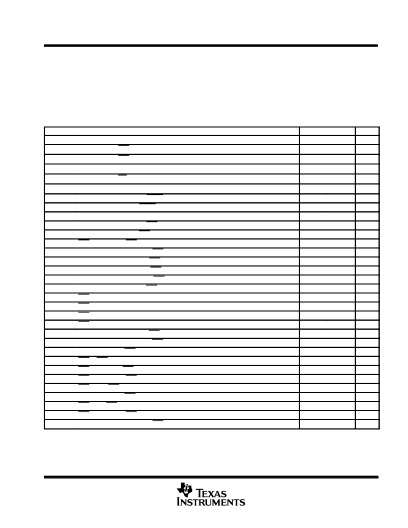
local-DRAM-bus timing
Local-DRAM-bus timing is specified differently than the other timing parameters. The DRAM interface times are
specified at 0.8 V and 2.4 V instead of at 1.5 V. This allows the designer to cross reference ’AV220 timing values
to DRAM specifications easily.
timing requirements and switching characteristics over recommended ranges of supply voltage
and operating free-air temperature range (unless otherwise noted)
local DRAM timing (see Note 5, Figure 17, and Figure 18)
MIN
MAX
UNIT
tc
tpd3
tpd4
tpd5
tpd6
tpd7
tsu8
th2
tASR
tDS
tDH
tRSH
tRRH
tRCS
tASC
tCAH
tRAH
tCAS
tCP
tRP
tRAS
tWCS
tWCH
tCAL
tRCD
tCSR
tCHR
tRPC
tRAL
tCSH
tRHCP
tRCH
NOTES:
SYSCLK period
25
ns
SYSCLK high to RAS low (see Note 6)
30
ns
SYSCLK high to CAS high (see Note 6)
25
ns
SYSCLK high to memory data high or low (DRAM write) (see Note 6)
30
ns
SYSCLK high to WE high or low (see Note 6)
22
ns
SYSCLK high to memory address high or low (see Note 6)
24
ns
Read data setup time before CASIN high
5
ns
Read data hold time after CASIN high
5
ns
Row address setup time (see Note 5)
tc–10
tc–15
tc–10
tc–5
tc–15
5tc–10
tc–15
tc–10
2tc–15
tc–5
tc–10
3tc–5
4tc–15
2tc–15
2tc–10
2tc–5
3tc–15
tc–10
3tc–15
2tc–10
2tc–10
4tc–15
2tc–5
tc–15
ns
Write data setup time before CAS low (see Note 6)
ns
Write data hold time after CAS low (see Note 6)
ns
RAS hold time after CAS low (see Note 6)
ns
Read command hold time from RAS high (see Note 6)
ns
Read command setup time to CAS low (see Note 6)
ns
Column address setup time to CAS low (see Note 6)
ns
Column address hold time from CAS low (see Note 6)
ns
Row address hold time from RAS low (see Note 6)
ns
CAS low time (see Note 6)
ns
CAS high time (see Note 6)
ns
RAS high time (see Note 6)
ns
RAS low time (see Note 6)
ns
Write command setup time to CAS low (see Note 6)
ns
Write command hold time from CAS low (see Note 6)
ns
Column address to CAS high (see Note 6)
ns
RAS to CAS delay (see Note 6)
ns
CAS setup time to RAS (memory refresh cycle) (see Note 6)
ns
CAS hold time from RAS (memory refresh cycle) (see Note 6)
ns
RAS high to CAS low delay (memory refresh cycle) (see Note 6)
ns
Column address to RAS high (see Note 6)
ns
RAS low to CAS high (see Note 6)
ns
RAS hold time from CAS precharge (see Note 6)
ns
Read command hold time from CAS high
ns
5. Not 100% tested, specified by design and characterization
6. MD15–MD0 are driven only when next cycle is a write.
相關(guān)PDF資料 |
PDF描述 |
|---|---|
| TMS320AV410 | Digital NTSC/PAL Encoder(數(shù)字NTSC/PAL編碼器) |
| TMS320AV411 | Digital NTSC/PAL Encoder(數(shù)字NTSC/PAL編碼器) |
| TMS320AV420 | Digital NTSC Encoder(數(shù)字NTSC編碼器) |
| TMS320C6424_1 | Fixed-Point Digital Signal Processor |
| TMS320C6455ZTZ | Fixed-Point Digital Signal Processor |
相關(guān)代理商/技術(shù)參數(shù) |
參數(shù)描述 |
|---|---|
| TMS320AV220PCM | 制造商:未知廠家 制造商全稱:未知廠家 功能描述:Audio/Video Decoder for MPEG |
| TMS320AV410 | 制造商:未知廠家 制造商全稱:未知廠家 功能描述:Color Encoder Circuit |
| TMS320AV410PJM | 制造商:Rochester Electronics LLC 功能描述:- Bulk |
| TMS320AV411 | 制造商:未知廠家 制造商全稱:未知廠家 功能描述:Color Encoder Circuit |
| TMS320AV411PJM | 制造商:Rochester Electronics LLC 功能描述:- Bulk 制造商:Texas Instruments 功能描述: |
發(fā)布緊急采購,3分鐘左右您將得到回復(fù)。