- 您現(xiàn)在的位置:買賣IC網(wǎng) > PDF目錄300033 > TMP89FH42UG 8-BIT, FLASH, 10 MHz, MICROCONTROLLER, PQFP44 PDF資料下載
參數(shù)資料
| 型號(hào): | TMP89FH42UG |
| 元件分類: | 微控制器/微處理器 |
| 英文描述: | 8-BIT, FLASH, 10 MHz, MICROCONTROLLER, PQFP44 |
| 封裝: | 10 X 10 MM, 0.80 MM PITCH, LEAD FREE, PLASTIC, LQFP-44 |
| 文件頁(yè)數(shù): | 272/317頁(yè) |
| 文件大小: | 6434K |
| 代理商: | TMP89FH42UG |
第1頁(yè)第2頁(yè)第3頁(yè)第4頁(yè)第5頁(yè)第6頁(yè)第7頁(yè)第8頁(yè)第9頁(yè)第10頁(yè)第11頁(yè)第12頁(yè)第13頁(yè)第14頁(yè)第15頁(yè)第16頁(yè)第17頁(yè)第18頁(yè)第19頁(yè)第20頁(yè)第21頁(yè)第22頁(yè)第23頁(yè)第24頁(yè)第25頁(yè)第26頁(yè)第27頁(yè)第28頁(yè)第29頁(yè)第30頁(yè)第31頁(yè)第32頁(yè)第33頁(yè)第34頁(yè)第35頁(yè)第36頁(yè)第37頁(yè)第38頁(yè)第39頁(yè)第40頁(yè)第41頁(yè)第42頁(yè)第43頁(yè)第44頁(yè)第45頁(yè)第46頁(yè)第47頁(yè)第48頁(yè)第49頁(yè)第50頁(yè)第51頁(yè)第52頁(yè)第53頁(yè)第54頁(yè)第55頁(yè)第56頁(yè)第57頁(yè)第58頁(yè)第59頁(yè)第60頁(yè)第61頁(yè)第62頁(yè)第63頁(yè)第64頁(yè)第65頁(yè)第66頁(yè)第67頁(yè)第68頁(yè)第69頁(yè)第70頁(yè)第71頁(yè)第72頁(yè)第73頁(yè)第74頁(yè)第75頁(yè)第76頁(yè)第77頁(yè)第78頁(yè)第79頁(yè)第80頁(yè)第81頁(yè)第82頁(yè)第83頁(yè)第84頁(yè)第85頁(yè)第86頁(yè)第87頁(yè)第88頁(yè)第89頁(yè)第90頁(yè)第91頁(yè)第92頁(yè)第93頁(yè)第94頁(yè)第95頁(yè)第96頁(yè)第97頁(yè)第98頁(yè)第99頁(yè)第100頁(yè)第101頁(yè)第102頁(yè)第103頁(yè)第104頁(yè)第105頁(yè)第106頁(yè)第107頁(yè)第108頁(yè)第109頁(yè)第110頁(yè)第111頁(yè)第112頁(yè)第113頁(yè)第114頁(yè)第115頁(yè)第116頁(yè)第117頁(yè)第118頁(yè)第119頁(yè)第120頁(yè)第121頁(yè)第122頁(yè)第123頁(yè)第124頁(yè)第125頁(yè)第126頁(yè)第127頁(yè)第128頁(yè)第129頁(yè)第130頁(yè)第131頁(yè)第132頁(yè)第133頁(yè)第134頁(yè)第135頁(yè)第136頁(yè)第137頁(yè)第138頁(yè)第139頁(yè)第140頁(yè)第141頁(yè)第142頁(yè)第143頁(yè)第144頁(yè)第145頁(yè)第146頁(yè)第147頁(yè)第148頁(yè)第149頁(yè)第150頁(yè)第151頁(yè)第152頁(yè)第153頁(yè)第154頁(yè)第155頁(yè)第156頁(yè)第157頁(yè)第158頁(yè)第159頁(yè)第160頁(yè)第161頁(yè)第162頁(yè)第163頁(yè)第164頁(yè)第165頁(yè)第166頁(yè)第167頁(yè)第168頁(yè)第169頁(yè)第170頁(yè)第171頁(yè)第172頁(yè)第173頁(yè)第174頁(yè)第175頁(yè)第176頁(yè)第177頁(yè)第178頁(yè)第179頁(yè)第180頁(yè)第181頁(yè)第182頁(yè)第183頁(yè)第184頁(yè)第185頁(yè)第186頁(yè)第187頁(yè)第188頁(yè)第189頁(yè)第190頁(yè)第191頁(yè)第192頁(yè)第193頁(yè)第194頁(yè)第195頁(yè)第196頁(yè)第197頁(yè)第198頁(yè)第199頁(yè)第200頁(yè)第201頁(yè)第202頁(yè)第203頁(yè)第204頁(yè)第205頁(yè)第206頁(yè)第207頁(yè)第208頁(yè)第209頁(yè)第210頁(yè)第211頁(yè)第212頁(yè)第213頁(yè)第214頁(yè)第215頁(yè)第216頁(yè)第217頁(yè)第218頁(yè)第219頁(yè)第220頁(yè)第221頁(yè)第222頁(yè)第223頁(yè)第224頁(yè)第225頁(yè)第226頁(yè)第227頁(yè)第228頁(yè)第229頁(yè)第230頁(yè)第231頁(yè)第232頁(yè)第233頁(yè)第234頁(yè)第235頁(yè)第236頁(yè)第237頁(yè)第238頁(yè)第239頁(yè)第240頁(yè)第241頁(yè)第242頁(yè)第243頁(yè)第244頁(yè)第245頁(yè)第246頁(yè)第247頁(yè)第248頁(yè)第249頁(yè)第250頁(yè)第251頁(yè)第252頁(yè)第253頁(yè)第254頁(yè)第255頁(yè)第256頁(yè)第257頁(yè)第258頁(yè)第259頁(yè)第260頁(yè)第261頁(yè)第262頁(yè)第263頁(yè)第264頁(yè)第265頁(yè)第266頁(yè)第267頁(yè)第268頁(yè)第269頁(yè)第270頁(yè)第271頁(yè)當(dāng)前第272頁(yè)第273頁(yè)第274頁(yè)第275頁(yè)第276頁(yè)第277頁(yè)第278頁(yè)第279頁(yè)第280頁(yè)第281頁(yè)第282頁(yè)第283頁(yè)第284頁(yè)第285頁(yè)第286頁(yè)第287頁(yè)第288頁(yè)第289頁(yè)第290頁(yè)第291頁(yè)第292頁(yè)第293頁(yè)第294頁(yè)第295頁(yè)第296頁(yè)第297頁(yè)第298頁(yè)第299頁(yè)第300頁(yè)第301頁(yè)第302頁(yè)第303頁(yè)第304頁(yè)第305頁(yè)第306頁(yè)第307頁(yè)第308頁(yè)第309頁(yè)第310頁(yè)第311頁(yè)第312頁(yè)第313頁(yè)第314頁(yè)第315頁(yè)第316頁(yè)第317頁(yè)
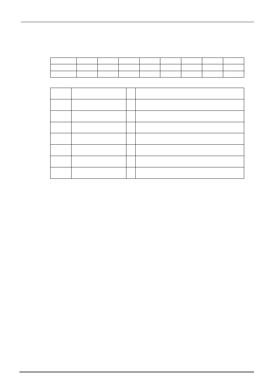
Internal factor reset detection status register
IRSTSR
(0x0FCC)
7
6
5
4
3
2
1
0
Bit Symbol
FCLR
FLSRF
TRMDS
TRMRF
LVD2RF
LVD1RF
SYSRF
WDTRF
Read/Write
W
R
After reset
0
FCLR
Flag initialization control
0 :
1 :
-
Clears the internal factor reset flag to "0".
FLSRF
Flash standby reset detection flag
0 :
1 :
-
Detects the flash standby reset.
TRMDS
Trimming data status
0 :
1 :
-
Detect state of abnormal trimming data
TRMRF
Trimming data reset detection flag
0 :
1 :
-
Detects the trimming data reset.
LVD2RF
Voltage detection reset 2 detection
flag
0 :
1 :
-
Detects the voltage detection 2 reset.
LVD1RF
Voltage detection reset 1 detection
flag
0 :
1 :
-
Detects the voltage detection 1 reset.
SYSRF
System clock reset detection flag
0 :
1 :
-
Detects the system clock reset.
WDTRF
Watchdog timer reset detection flag
0 :
1 :
-
Detects the watchdog timer reset.
Note 1: Internal reset factor flag (IRSTSR<FLSRF, TRMDS, TRMRF, LVD2RF, LVD1RF, SYSRF, WDTRF>) is initialized only by
a power-on reset, an external reset input or IRSTSR <FCLR>. It is not initialized by an internal factor reset.
Note 2: Care must be taken in system designing since the IRSTSR may not fulfill its functions due to disturbing noise and other
effects.
Note 3: If SYSCR4 is set to 0x71 after IRSTSR<FCLR> is set to "1", internal factor reset flag is cleared to "0" and IRSTSR<FCLR>
is automatically cleared to "0".
Note 4: After IRSTSR<FCLR> is modified, SYSCR4 should be written 0x71 (Enable code for IRSTSR<FCLR> in NORMAL mode
when fcgck is fc/4 (CGCR<FCGCKSEL>=00). Otherwise, IRSTSR<FCLR> may be enabled at unexpected timing.
Note 5: Bit 7 of IRSTSR is read as "0".
2.4.3
Functions
The power-on reset, external reset input and internal factor reset signals are input to the warm-up circuit of the
clock generator.
During reset, the warm-up counter circuit is reset, and the CPU and the peripheral circuits are reset.
After reset is released, the warm-up counter starts counting the high frequency clock (fc), and executes the
warm-up operation that follows reset release.
During the warm-up operation that follows reset release, the trimming data is loaded from the non-volatile
exclusive use memory for adjustment of the ladder resistor that generates the comparison voltage for the power-
on reset and the voltage detection circuits.
When the warm-up operation that follows reset release is finished, the CPU starts execution of the program
from the reset vector address stored in addresses 0xFFFE to 0xFFFF.
When a reset signal is input during the warm-up operation that follows reset release, the warm-up counter
circuit is reset.
The reset operation is common to the power-on reset, external reset input and internal factor resets, except for
the initialization of some special function registers and the initialization of the voltage detection circuits.
When a reset is applied, the peripheral circuits become the states as shown in Table 2-5.
TMP89FH42
2. CPU Core
2.4 Reset Control Circuit
Page 42
RA004
相關(guān)PDF資料 |
PDF描述 |
|---|---|
| TMP91FW60FG | MICROCONTROLLER, PQFP100 |
| TMPG06-24A-4 | 400 W, UNIDIRECTIONAL, SILICON, TVS DIODE |
| TMPG06-8.2A-23 | 400 W, UNIDIRECTIONAL, SILICON, TVS DIODE |
| TMPZ5250LR | 20 V, SILICON, UNIDIRECTIONAL VOLTAGE REGULATOR DIODE, TO-236AB |
| TMPZ5233R | 6 V, SILICON, UNIDIRECTIONAL VOLTAGE REGULATOR DIODE, TO-236AA |
相關(guān)代理商/技術(shù)參數(shù) |
參數(shù)描述 |
|---|---|
| TMP89FH42UG(JZ) | 制造商:Toshiba America Electronic Components 功能描述:MCU 8BIT 16384BYTES FLASH 44LQFP |
| TMP89FH46 | 制造商:TOSHIBA 制造商全稱:Toshiba Semiconductor 功能描述:8 Bit Microcontroller |
| TMP89FH46DUG | 制造商:TOSHIBA 制造商全稱:Toshiba Semiconductor 功能描述:Microcomputers / Microcomputer Development Systems |
| TMP89FH46LDUG | 制造商:TOSHIBA 制造商全稱:Toshiba Semiconductor 功能描述:Microcomputers / Microcomputer Development Systems |
| TMP89FM40NG | 制造商:TOSHIBA 制造商全稱:Toshiba Semiconductor 功能描述:Microcomputers / Microcomputer Development Systems |
發(fā)布緊急采購(gòu),3分鐘左右您將得到回復(fù)。