- 您現(xiàn)在的位置:買賣IC網(wǎng) > PDF目錄98068 > S1C621C0D 4-BIT, MROM, 1.3 MHz, MICROCONTROLLER, UUC74 PDF資料下載
參數(shù)資料
| 型號: | S1C621C0D |
| 元件分類: | 微控制器/微處理器 |
| 英文描述: | 4-BIT, MROM, 1.3 MHz, MICROCONTROLLER, UUC74 |
| 封裝: | DIE-74 |
| 文件頁數(shù): | 34/108頁 |
| 文件大小: | 992K |
| 代理商: | S1C621C0D |
第1頁第2頁第3頁第4頁第5頁第6頁第7頁第8頁第9頁第10頁第11頁第12頁第13頁第14頁第15頁第16頁第17頁第18頁第19頁第20頁第21頁第22頁第23頁第24頁第25頁第26頁第27頁第28頁第29頁第30頁第31頁第32頁第33頁當(dāng)前第34頁第35頁第36頁第37頁第38頁第39頁第40頁第41頁第42頁第43頁第44頁第45頁第46頁第47頁第48頁第49頁第50頁第51頁第52頁第53頁第54頁第55頁第56頁第57頁第58頁第59頁第60頁第61頁第62頁第63頁第64頁第65頁第66頁第67頁第68頁第69頁第70頁第71頁第72頁第73頁第74頁第75頁第76頁第77頁第78頁第79頁第80頁第81頁第82頁第83頁第84頁第85頁第86頁第87頁第88頁第89頁第90頁第91頁第92頁第93頁第94頁第95頁第96頁第97頁第98頁第99頁第100頁第101頁第102頁第103頁第104頁第105頁第106頁第107頁第108頁
S1C621C0 TECHNICAL MANUAL
EPSON
23
CHAPTER 4: PERIPHERAL CIRCUITS AND OPERATION (Output Ports)
At initial reset, the output terminals are set to low (VSS).
When an R0x is used as the special output port, fix the output port register R0x at "0" and turn the signal
ON or OFF using the special output enable register.
Note: Be sure that the output terminal is fixed at a high (VDD) level the same with the DC output if "1" is
written to the R0x register when the special output has been selected.
REMCR (R00) and REMDC (R01) outputs
REMCR (remote control carrier) signal generated by the built-in remote controller can be output from the
R00 terminal.
This output signal is used to drive the LED for an infrared remote controller so that the remote control
signal is transmitted.
Similarly, REMDC (DC) signal that has not yet done pulse modulation can be output from the R01 termi-
nal.
When R00 is used for REMCR output, keep R00 register set to "0". The signal output can be controlled
using the REMCR register. When the REMCR register is set to "1", the REM (remote controller) circuit goes
on and shifts to the status in which the REMCR signal can be output from the R00 terminal. When "0" is set,
the R00 terminal goes low level (VSS).
When R01 is used for REMDC output, keep the R01 register set to "0". The signal output can be controlled
using the REMDC register. When the REMDC register is set to "1", the REM (remote controller) circuit goes
on and shifts to the status in which the REMDC signal can be output from the R01 terminal. When "0" is set,
the R01 terminal goes low level (VSS).
See Section 4.9, "Remote Controller (REM)" for the output waveform and output timing.
FOUT (R02)
In order for the S1C621C0 to provide clock signal to an external device, FOUT signal can be output from
the R02 terminal.
When R02 is used for FOUT output, keep R02 register set to "0". ON/OFF of the signal output can be
controlled using the FOUT output enable register FOUTE.
When the FOUTE register is set to "1", FOUT signal is output from the R02 terminal. When "0" is set, the
R02 terminal goes low level (VSS).
The frequency of clock output signal may be selected from among 4 types as Table 4.5.3.2 by setting of the
FOFQ0 and FOFQ1 registers.
Table 4.5.3.2 FOUT clock frequency
FOFQ1
0
1
FOFQ0
0
1
0
1
Clock frequency (Hz)
512
4,096
fOSC1
fOSC3
fOSC1: OSC1 oscillation frequency
fOSC3: OSC3 oscillation frequency
Note: A hazard may occur when the FOUT signal is turned ON or OFF.
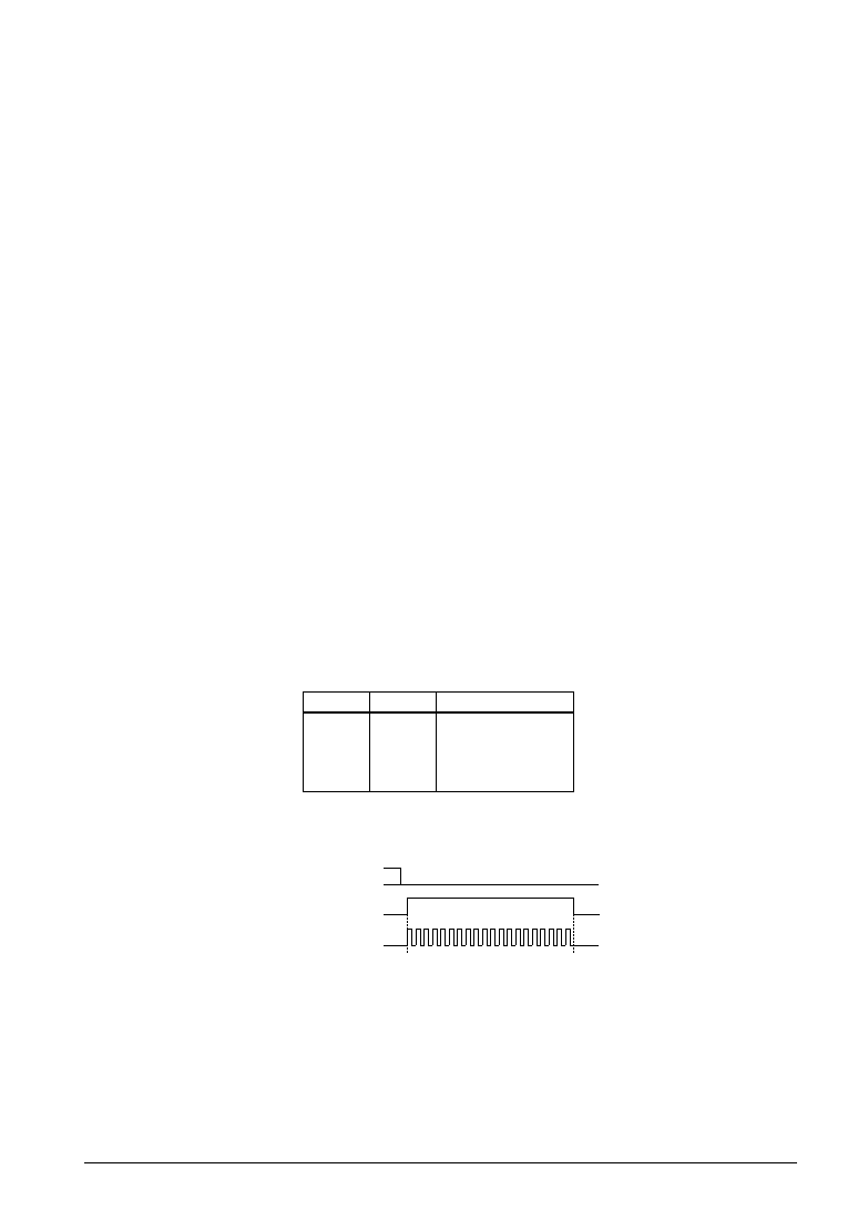
Figure 4.5.3.2 shows the output waveform of FOUT.
Fig. 4.5.3.2 Output waveform of FOUT
FOUTE register
FOUT output (R02)
01
R02 register
Fixed at 0
0
相關(guān)PDF資料 |
PDF描述 |
|---|---|
| S1C62480D | 4-BIT, MROM, 2.3 MHz, MICROCONTROLLER, UUC135 |
| S1C62440F | 4-BIT, MROM, 2.3 MHz, MICROCONTROLLER, PQFP128 |
| S1C62740D | 4-BIT, MROM, 1.3 MHz, MICROCONTROLLER, UUC109 |
| S1C62920D | 4-BIT, MROM, 1.3 MHz, MICROCONTROLLER, UUC63 |
| S1C62A33D | 4-BIT, MROM, 0.6 MHz, MICROCONTROLLER, UUC86 |
相關(guān)代理商/技術(shù)參數(shù) |
參數(shù)描述 |
|---|---|
| S1C63004 | 制造商:EPSON 制造商全稱:EPSON 功能描述:CMOS 4-bit Single Chip Microcontroller |
| S1C63008 | 制造商:EPSON 制造商全稱:EPSON 功能描述:CMOS 4-bit Single Chip Microcontroller |
| S1C63016 | 制造商:EPSON 制造商全稱:EPSON 功能描述:CMOS 4-bit Single Chip Microcontroller |
| S1C63158 | 制造商:EPSON 制造商全稱:EPSON 功能描述:4-bit Single Chip Microcomputer |
| S1C63408 | 制造商:EPSON 制造商全稱:EPSON 功能描述:4-bit Single Chip Microcomputer |
發(fā)布緊急采購,3分鐘左右您將得到回復(fù)。