- 您現(xiàn)在的位置:買賣IC網(wǎng) > PDF目錄98023 > ML671000 (LAPIS SEMICONDUCTOR CO LTD) 32-BIT, 24 MHz, RISC MICROCONTROLLER, PQFP128 PDF資料下載
參數(shù)資料
| 型號(hào): | ML671000 |
| 廠商: | LAPIS SEMICONDUCTOR CO LTD |
| 元件分類: | 微控制器/微處理器 |
| 英文描述: | 32-BIT, 24 MHz, RISC MICROCONTROLLER, PQFP128 |
| 封裝: | 14 X 20 MM, 0.50 MM PITCH, PLASTIC, QFP-128 |
| 文件頁數(shù): | 154/303頁 |
| 文件大?。?/td> | 1395K |
| 代理商: | ML671000 |
第1頁第2頁第3頁第4頁第5頁第6頁第7頁第8頁第9頁第10頁第11頁第12頁第13頁第14頁第15頁第16頁第17頁第18頁第19頁第20頁第21頁第22頁第23頁第24頁第25頁第26頁第27頁第28頁第29頁第30頁第31頁第32頁第33頁第34頁第35頁第36頁第37頁第38頁第39頁第40頁第41頁第42頁第43頁第44頁第45頁第46頁第47頁第48頁第49頁第50頁第51頁第52頁第53頁第54頁第55頁第56頁第57頁第58頁第59頁第60頁第61頁第62頁第63頁第64頁第65頁第66頁第67頁第68頁第69頁第70頁第71頁第72頁第73頁第74頁第75頁第76頁第77頁第78頁第79頁第80頁第81頁第82頁第83頁第84頁第85頁第86頁第87頁第88頁第89頁第90頁第91頁第92頁第93頁第94頁第95頁第96頁第97頁第98頁第99頁第100頁第101頁第102頁第103頁第104頁第105頁第106頁第107頁第108頁第109頁第110頁第111頁第112頁第113頁第114頁第115頁第116頁第117頁第118頁第119頁第120頁第121頁第122頁第123頁第124頁第125頁第126頁第127頁第128頁第129頁第130頁第131頁第132頁第133頁第134頁第135頁第136頁第137頁第138頁第139頁第140頁第141頁第142頁第143頁第144頁第145頁第146頁第147頁第148頁第149頁第150頁第151頁第152頁第153頁當(dāng)前第154頁第155頁第156頁第157頁第158頁第159頁第160頁第161頁第162頁第163頁第164頁第165頁第166頁第167頁第168頁第169頁第170頁第171頁第172頁第173頁第174頁第175頁第176頁第177頁第178頁第179頁第180頁第181頁第182頁第183頁第184頁第185頁第186頁第187頁第188頁第189頁第190頁第191頁第192頁第193頁第194頁第195頁第196頁第197頁第198頁第199頁第200頁第201頁第202頁第203頁第204頁第205頁第206頁第207頁第208頁第209頁第210頁第211頁第212頁第213頁第214頁第215頁第216頁第217頁第218頁第219頁第220頁第221頁第222頁第223頁第224頁第225頁第226頁第227頁第228頁第229頁第230頁第231頁第232頁第233頁第234頁第235頁第236頁第237頁第238頁第239頁第240頁第241頁第242頁第243頁第244頁第245頁第246頁第247頁第248頁第249頁第250頁第251頁第252頁第253頁第254頁第255頁第256頁第257頁第258頁第259頁第260頁第261頁第262頁第263頁第264頁第265頁第266頁第267頁第268頁第269頁第270頁第271頁第272頁第273頁第274頁第275頁第276頁第277頁第278頁第279頁第280頁第281頁第282頁第283頁第284頁第285頁第286頁第287頁第288頁第289頁第290頁第291頁第292頁第293頁第294頁第295頁第296頁第297頁第298頁第299頁第300頁第301頁第302頁第303頁
ML671000 User’s Manual
Chapter 12
External Memory Controller (XMC)
12-7
12.1.4. Address Space
Although the CPU architecture theoretically provides a 32-bit address space of 4 gigabytes, this LSI
ignores the top six bits (A31 to A26) and uses 26-bit addressing to access only the first 64
megabytes.
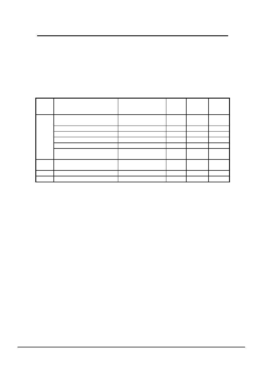
Table 12-3 outlines the memory types for the regions in these four 16-megabyte banks.
Table 12-3
Address Space Regions
Bank
Addresses
Assignment
Size
Chip
Select
Data
Bus
Width
0x00000000 to 0x001FFFFF
External ROM, RAM,
and peripherals
2MB
nCS0
8/16
0x00200000 to 0x003FFFFF
Internal RAM
2MB
-
32
0x00400000 to 0x005FFFFF
Core bus I/O space
2MB
-
32
0x00600000 to 0x006FFFFF
Peripheral bus I/O space
1MB
-
16
0x00700000 to 0x007FFFFF
Internal reserved region
1MB
-
16
0
0x00800000 to 0x00FFFFFF
External ROM, RAM,
and peripherals
8MB
nCS0
8/16
1
0x01000000 to 0x01FFFFFF
External ROM, RAM,
and peripherals
16MB
nCS1
8/16
2
0x02000000 to 0x02FFFFFF
External DRAM
16MB
nRAS0
8/16
3
0x03000000 to 0x03FFFFFF
External DRAM
16MB
nRAS1
8/16
The 64-megabyte address space is divided into four 16-megabyte banks specified by the top two
address bits (A25 and A24).
Each bank is assigned a specific type and provides the appropriate strobe signals to enable the direct
connection of memory and peripheral devices of that type.
Bank 0 is further divided in the following regions.
0x00000000 to 0x001FFFFF External memory (ROM, RAM, and peripherals)
0x00200000 to 0x003FFFFF Internal RAM. Only 4 kilobytes (0x00200000 to 0x00200FFF) is
physically present.
0x00400000 to 0x005FFFFF Core bus I/O space. This contains the CPU control block control
registers.
0x00600000 to 0x006FFFFF Peripheral bus I/O space. This contains the control registers for all on-
chip peripherals outside the CPU control block.
0x00700000 to 0x007FFFFF Reserved space not available for use.
0x00800000 to 0x00FFFFFF External memory (ROM, RAM, and peripherals)
Do not access bank 0 addresses between 0x00200000 to 0x006FFFFF that do not have internal RAM
or a control register physically present. Operation is not guaranteed.
Bank 1 is accessed as an external memory space for ROM, RAM, and I/O; banks 2 and 3, as external
DRAM spaces.
Bank 2 or 3 access uses the output signals nRAS, nCAS, and a multiplexed address.
Each bank has its own bus width setting (8 or 16 bits).
Figure 12-2 shows the address space.
相關(guān)PDF資料 |
PDF描述 |
|---|---|
| ML87V3104 | 2048 X 1024 DOTS DOT MAT LCD DSPL CTLR, PQFP100 |
| ML9203-XXGA | 16 X 35 DOTS FLUORESCENT DSPL CTRL, PQFP100 |
| ML9204-XXGA | 24 X 35 DOTS FLUORESCENT DSPL CTRL, PQFP128 |
| ML9205-01GA | 24 X 39 DOTS FLUORESCENT DSPL CTRL, PQFP80 |
| ML9620GAZ210 | 1 CHANNEL(S), 1M bps, LOCAL AREA NETWORK CONTROLLER, PQFP44 |
相關(guān)代理商/技術(shù)參數(shù) |
參數(shù)描述 |
|---|---|
| ML671000GA | 制造商:OK International 功能描述:CMOS 32-Bit Single-Chip Microcontroller with Built-in USB Device Controller |
| ML672 | 制造商:PYRAMID 制造商全稱:Pyramid Semiconductor Corporation 功能描述:Quad 2-Input “Nand” Gate |
| ML674000 | 制造商:OKI 制造商全稱:OKI electronic componets 功能描述:32-bit General-purpose, ARM-based Microcontroller |
| ML674000-KIT | 制造商:ROHM Semiconductor 功能描述:CMOS 32-Bit ARM-Based General-Purpose Single-Chip Microcontroller |
| ML674000LA | 制造商:ROHM Semiconductor 功能描述:ML674000LAZ03A |
發(fā)布緊急采購,3分鐘左右您將得到回復(fù)。