- 您現(xiàn)在的位置:買賣IC網(wǎng) > PDF目錄384544 > ISPCLOCK5600 (Lattice Semiconductor Corporation) In-System Programmable, Zero-Delay Clock Generator with Universal Fan-Out Buffer PDF資料下載
參數(shù)資料
| 型號: | ISPCLOCK5600 |
| 廠商: | Lattice Semiconductor Corporation |
| 英文描述: | In-System Programmable, Zero-Delay Clock Generator with Universal Fan-Out Buffer |
| 中文描述: | 在系統(tǒng)可編程,零延遲時鐘發(fā)生器通用扇出緩沖器 |
| 文件頁數(shù): | 25/47頁 |
| 文件大?。?/td> | 871K |
| 代理商: | ISPCLOCK5600 |
第1頁第2頁第3頁第4頁第5頁第6頁第7頁第8頁第9頁第10頁第11頁第12頁第13頁第14頁第15頁第16頁第17頁第18頁第19頁第20頁第21頁第22頁第23頁第24頁當(dāng)前第25頁第26頁第27頁第28頁第29頁第30頁第31頁第32頁第33頁第34頁第35頁第36頁第37頁第38頁第39頁第40頁第41頁第42頁第43頁第44頁第45頁第46頁第47頁
Lattice Semiconductor
ispClock5600 Family Data Sheet
25
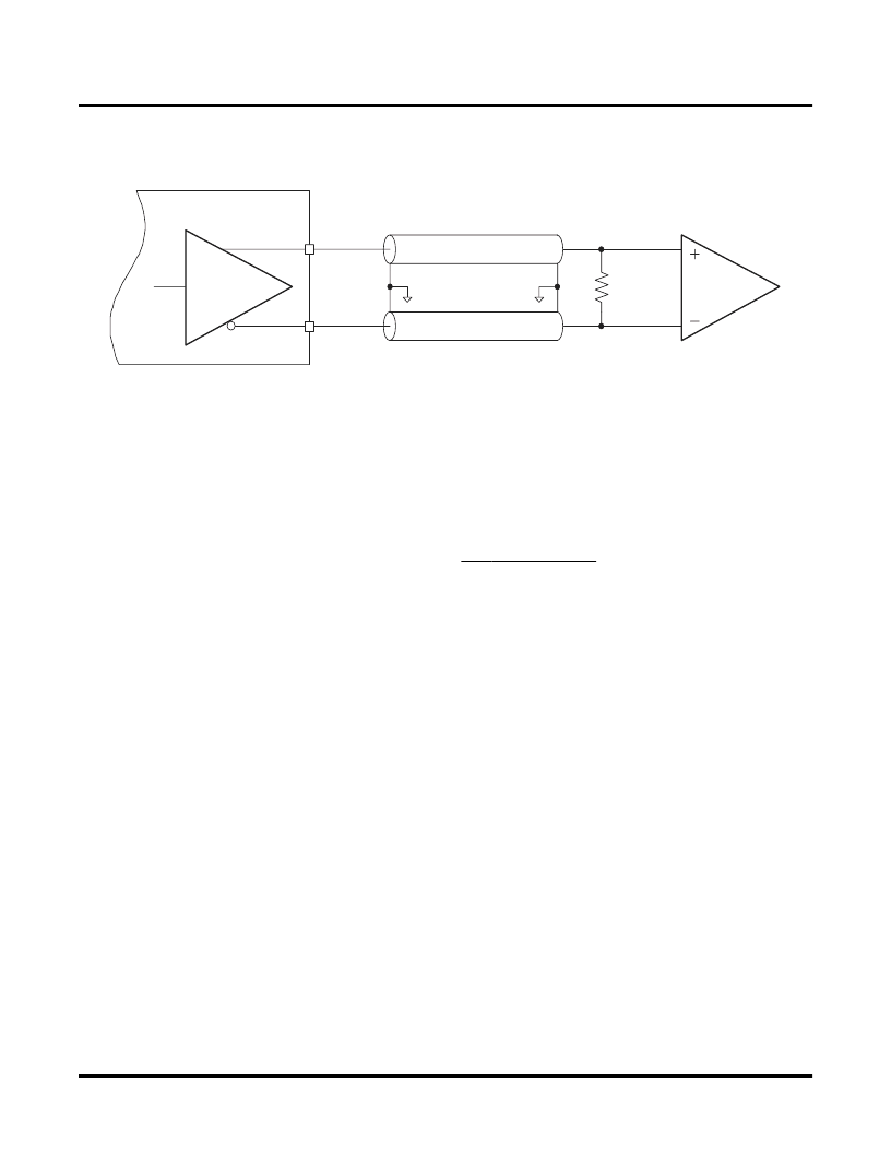
LVPECL mode. The far end of the transmission line must be terminated with a 100
resistor across the two signal
lines.
Figure 22. Configuration for LVDS and LVPECL Output Modes
Note that when in LVPECL output mode, the ispClock5600’s output driver provides an internal pull-down, unlike a
typical bipolar LVPECL driver. For this reason no external pull-down resistors are necessary and the driver may be
terminated with a single 100
resistor across the signal lines. For proper operation, pull-down resistors should
NOT be used with the ispClock5600’s LVPECL output mode.
Thermal Management
In applications where a majority of the ispClock5610 or ispClock5620’s outputs are active and operating at or near
maximum output frequency (320 MHz), package thermal limitations may need to be considered to ensure a suc-
cessful design. Thermal characteristics of the packages employed by Lattice Semiconductor may be found in the
document
Thermal Management
which may be obtained at www.latticesemi.com.
The maximum current consumption of the digital and analog core circuitry is approximately 167mA worst case
(I
CCD
+ I
CCA
), and each of the output banks may draw up to 35mA worst case (LVCMOS 3.3V, CL=18pF, f
OUT
=320
MHz, both outputs in each bank enabled). This results in a total device dissipation:
P
DMAX
= 3.3V x (10 x 35mA + 167mA) = 1.7W
(3)
With a maximum recommended operating junction temperature (T
JOP
) of 115°C for an industrial grade device, the
maximum allowable ambient temperature (T
AMAX
) can be estimated as
T
AMAX
= T
JOP
- PD
MAX
x
Θ
JA
= 115°C - 1.7W x 35°C/W = 55°C
(4)
where
Θ
JA
= 35 °C/W in still air for the ispClock5620’s TQFP100 package.
The above analysis represents the worst-case scenario. Signi
fi
cant improvement in maximum ambient operating
temperature can be realized with additional cooling. Providing a 200 LFM (Linear Feet per Minute) air
fl
ow reduces
Θ
JA
to 29°C/W, which results in a maximum ambient operating temperature of 66°C.
In practice, however, the absolute worst-case situation will be relatively rare, as not all outputs may be running at
maximum output frequency in a given application. Additionally, if the internal VCO is operating at less than its max-
imum frequency (640MHz), it requires less current on the VCCD pin. In these situations, one can estimate the
effective I
CCO
for each bank and the effective I
CCD
for the digital core functions based on output frequency and
VCO frequency. Normalized curves relating current to operating frequency for these parameters may be found in
the Typical Performance Characteristics section.
While it is possible to perform detailed calculations to estimate the maximum ambient operating temperature from
operating conditions, some simpler rule-of-thumb guidance can also be obtained through the derating curves
shown in Figure 23. The curves in Figure 23a show the maximum ambient operating temperature permitted when
operating a given number of output banks at the maximum output frequency (320MHz). Note that it is assumed that
both outputs in each bank are active.
Zo=50
ispClock5600
LVDS/LVPECL
mode
LVDS/PECL
Receiver
RT=100
Zo=50
相關(guān)PDF資料 |
PDF描述 |
|---|---|
| ISPPAC-CLK5610V-01T100C | In-System Programmable, Zero-Delay Clock Generator with Universal Fan-Out Buffer |
| ISPPAC-CLK5620V-01T100C | LED Area Light; LED Color:Blue; Leaded Process Compatible:No; Light Emitting Area:80x80mm; Peak Reflow Compatible (260 C):No; Supply Current:250mA; Supply Voltage:24VDC; Wavelength:470nm |
| ISPPAC-CLK5620V-01T100I | In-System Programmable, Zero-Delay Clock Generator with Universal Fan-Out Buffer |
| ISPPAC-CLK5610V-01T48C | Spot Light; LED Color:Blue; Leaded Process Compatible:No; Peak Reflow Compatible (260 C):No; Supply Current:160mA; Supply Voltage:30VDC; Wavelength:470nm |
| ISPPAC-CLK5620V-01T48C | LED Area Light; LED Color:Green; Leaded Process Compatible:No; Light Emitting Area:62x62mm; Peak Reflow Compatible (260 C):No; Supply Current:200mA; Supply Voltage:24VDC; Wavelength:525nm |
相關(guān)代理商/技術(shù)參數(shù) |
參數(shù)描述 |
|---|---|
| ISPCLOCK5600A | 制造商:LATTICE 制造商全稱:Lattice Semiconductor 功能描述:In-System Programmable, Enhanced Zero-Delay, Clock Generator with Universal Fan-Out Buffer |
| ISPCLOCK5610A | 制造商:LATTICE 制造商全稱:Lattice Semiconductor 功能描述:In-System Programmable, Enhanced Zero-Delay, Clock Generator with Universal Fan-Out Buffer |
| ISPCLOCK5620A | 制造商:LATTICE 制造商全稱:Lattice Semiconductor 功能描述:In-System Programmable, Enhanced Zero-Delay, Clock Generator with Universal Fan-Out Buffer |
| ISPD60 | 制造商:未知廠家 制造商全稱:未知廠家 功能描述:DARLINGTON-NPN-OUTPUT DC-INPUT OPTOCOUPLER |
| ISPD60_10 | 制造商:ISOCOM 制造商全稱:ISOCOM 功能描述:NON BASE LEAD OPTICALLY COUPLED ISOLATOR PHOTODARLINGTON OUTPUT |
發(fā)布緊急采購,3分鐘左右您將得到回復(fù)。