- 您現(xiàn)在的位置:買賣IC網 > PDF目錄1915 > DS32512N+ (Maxim Integrated Products)IC LIU DS3/E3/STS-1 12P 484-BGA PDF資料下載
參數資料
| 型號: | DS32512N+ |
| 廠商: | Maxim Integrated Products |
| 文件頁數: | 60/130頁 |
| 文件大?。?/td> | 0K |
| 描述: | IC LIU DS3/E3/STS-1 12P 484-BGA |
| 產品培訓模塊: | Lead (SnPb) Finish for COTS Obsolescence Mitigation Program |
| 標準包裝: | 30 |
| 類型: | 線路接口裝置(LIU) |
| 規(guī)程: | DS3 |
| 電源電壓: | 3.135 V ~ 3.465 V |
| 安裝類型: | 表面貼裝 |
| 封裝/外殼: | 484-BGA |
| 供應商設備封裝: | 484-BGA(23x23) |
| 包裝: | 管件 |
第1頁第2頁第3頁第4頁第5頁第6頁第7頁第8頁第9頁第10頁第11頁第12頁第13頁第14頁第15頁第16頁第17頁第18頁第19頁第20頁第21頁第22頁第23頁第24頁第25頁第26頁第27頁第28頁第29頁第30頁第31頁第32頁第33頁第34頁第35頁第36頁第37頁第38頁第39頁第40頁第41頁第42頁第43頁第44頁第45頁第46頁第47頁第48頁第49頁第50頁第51頁第52頁第53頁第54頁第55頁第56頁第57頁第58頁第59頁當前第60頁第61頁第62頁第63頁第64頁第65頁第66頁第67頁第68頁第69頁第70頁第71頁第72頁第73頁第74頁第75頁第76頁第77頁第78頁第79頁第80頁第81頁第82頁第83頁第84頁第85頁第86頁第87頁第88頁第89頁第90頁第91頁第92頁第93頁第94頁第95頁第96頁第97頁第98頁第99頁第100頁第101頁第102頁第103頁第104頁第105頁第106頁第107頁第108頁第109頁第110頁第111頁第112頁第113頁第114頁第115頁第116頁第117頁第118頁第119頁第120頁第121頁第122頁第123頁第124頁第125頁第126頁第127頁第128頁第129頁第130頁
DS32506/DS32508/DS32512
35 of 130
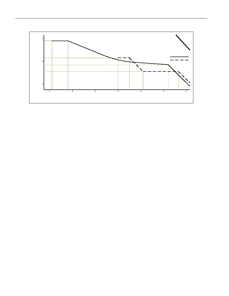
Figure 8-6. DS3 and E3 Wander Tolerance
10
100
0.13
DS325xx
Wander Tolerance
Wan
der
Tole
ra
nc
e(UI
p-
p)
Frequency (Hz)
1
1000
4.4
34.4
10-1
10-2
137.5
0.032
G.823 (E3)
G.824 (DS3)
67
1.675
805
10-3
10-4
10-5
1.2
6.12
8.3.10 Jitter Transfer
Without the jitter attenuator on the receive side, the receiver attenuates jitter at frequencies above its corner
frequency (approximately 300kHz) and passes jitter at lower frequencies. With the jitter attenuator enabled on the
receive side, the receiver meets the jitter transfer requirements of all applicable telecommunication standards in
Table 1-1. See Figure 8-7.
8.4 Jitter Attenuator
Each LIU contains an on-board jitter attenuator that can be placed in the receive path or the transmit path or can
be disabled. When only the hardware interface is enabled (IFSEL = 000 and HW = 1), the JAS[1:0] and JAD[1:0]
pins specify the specify the JA location and buffer depth for all ports. When a microprocessor interface is enabled
≠ 000), the JAS[1:0] and JAD[1:0] pins are ignored, and the LIU.CR1:JAS[1:0] and JAD[1:0] configuration
bits specify the JA location and buffer depth for each port individually. The JA buffer depth can be set to 16, 32, 64
or 128 bits. Figure 8-7 shows the minimum jitter attenuation for the device when the jitter attenuator is enabled.
Figure 8-7 also shows the receive jitter transfer when the jitter attenuator is disabled.
The jitter attenuator consists of a narrowband PLL to retime the selected clock, a FIFO to buffer the associated
data while the clock is being retimed, and logic to prevent FIFO over/underflow in the presence of very large jitter
amplitudes. The JA has a loop bandwidth of reference_clock
÷ 2,058,874 (see corner frequencies in Figure 8-7).
The JA attenuates jitter at frequencies higher than the loop bandwidth, while allowing jitter (and wander) at lower
frequencies to pass through relatively unaffected.
The jitter attenuator requires a transmission-quality reference clock (i.e.,
±20ppm frequency accuracy and low
jitter). See Section 8.7.1 for more information about reference clocks and clock selection.
When the microprocessor interface is enabled, the jitter attenuator indicates the fill status of its FIFO buffer in the
LIU.SRL:JAFL (JA full) and LIU.SRL:JAEL (JA empty) status bits. When the buffer becomes full, the JA
momentarily increases the frequency of the read clock by 6250ppm to avoid buffer overflow and consequent data
errors. When the buffer becomes empty, the JA momentarily decreases the frequency of the read clock by
6250ppm to avoid buffer underflow and consequent data errors. During these momentary frequency adjustments,
jitter is passed through the JA to avoid over/underflow. If the phase noise or frequency offset of the write clock is
large enough to cause the buffer to overflow or underflow, the JA sets both the JAFL bit and the JAEL bit to
indicate that data errors have occurred. JAFL and JAEL can cause an interrupt if enabled by the corresponding
enable bits in the LIU.SRIE register.
As shown in Figure 8-7, the jitter attenuator meets the jitter transfer requirements of all applicable standards listed
in Table 1-1.
相關PDF資料 |
PDF描述 |
|---|---|
| DS3254N+ | IC LIU DS3/E3/STS-1 144-CSBGA |
| DS33M33N+ | IC MAPPER ETHERNET 256CSBGA |
| DS33R11+CJ2 | IC ETH TXRX T1/E1/J1 256-BGA |
| DS33R41+ | IC TXRX ETHERNET MAP 400-BGA |
| DS33W11DK+ | IC MAPPING ETHERNET 256-CSBGA |
相關代理商/技術參數 |
參數描述 |
|---|---|
| DS32512N# | 功能描述:網絡控制器與處理器 IC 12-Port DS3/E3/STS-1 Line Interface Unit RoHS:否 制造商:Micrel 產品:Controller Area Network (CAN) 收發(fā)器數量: 數據速率: 電源電流(最大值):595 mA 最大工作溫度:+ 85 C 安裝風格:SMD/SMT 封裝 / 箱體:PBGA-400 封裝:Tray |
| DS32512N+ | 功能描述:網絡控制器與處理器 IC 12-Port DS3/E3/STS-1 Line Interface Unit RoHS:否 制造商:Micrel 產品:Controller Area Network (CAN) 收發(fā)器數量: 數據速率: 電源電流(最大值):595 mA 最大工作溫度:+ 85 C 安裝風格:SMD/SMT 封裝 / 箱體:PBGA-400 封裝:Tray |
| DS32512NA2 | 制造商:Maxim Integrated Products 功能描述:DS32512 X12 DS3/E3 LIU REVA2 IND - Rail/Tube |
| DS32512NW | 功能描述:網絡控制器與處理器 IC RoHS:否 制造商:Micrel 產品:Controller Area Network (CAN) 收發(fā)器數量: 數據速率: 電源電流(最大值):595 mA 最大工作溫度:+ 85 C 安裝風格:SMD/SMT 封裝 / 箱體:PBGA-400 封裝:Tray |
| DS32512W | 功能描述:網絡控制器與處理器 IC RoHS:否 制造商:Micrel 產品:Controller Area Network (CAN) 收發(fā)器數量: 數據速率: 電源電流(最大值):595 mA 最大工作溫度:+ 85 C 安裝風格:SMD/SMT 封裝 / 箱體:PBGA-400 封裝:Tray |
發(fā)布緊急采購,3分鐘左右您將得到回復。