- 您現(xiàn)在的位置:買賣IC網(wǎng) > PDF目錄4285 > XC2S150E-6FT256I (Xilinx Inc)SPARTAN FPGA 150000 GATE 1.8V PDF資料下載
參數(shù)資料
| 型號: | XC2S150E-6FT256I |
| 廠商: | Xilinx Inc |
| 文件頁數(shù): | 38/108頁 |
| 文件大小: | 0K |
| 描述: | SPARTAN FPGA 150000 GATE 1.8V |
| 產(chǎn)品變化通告: | FPGA Family Discontinuation 18/Apr/2011 |
| 標準包裝: | 90 |
| 系列: | Spartan®-IIE |
| LAB/CLB數(shù): | 864 |
| 邏輯元件/單元數(shù): | 3888 |
| RAM 位總計: | 49152 |
| 輸入/輸出數(shù): | 182 |
| 門數(shù): | 150000 |
| 電源電壓: | 1.71 V ~ 1.89 V |
| 安裝類型: | 表面貼裝 |
| 工作溫度: | -40°C ~ 100°C |
| 封裝/外殼: | 256-LBGA |
| 供應(yīng)商設(shè)備封裝: | 256-FTBGA |
| 其它名稱: | Q1280323 |
第1頁第2頁第3頁第4頁第5頁第6頁第7頁第8頁第9頁第10頁第11頁第12頁第13頁第14頁第15頁第16頁第17頁第18頁第19頁第20頁第21頁第22頁第23頁第24頁第25頁第26頁第27頁第28頁第29頁第30頁第31頁第32頁第33頁第34頁第35頁第36頁第37頁當(dāng)前第38頁第39頁第40頁第41頁第42頁第43頁第44頁第45頁第46頁第47頁第48頁第49頁第50頁第51頁第52頁第53頁第54頁第55頁第56頁第57頁第58頁第59頁第60頁第61頁第62頁第63頁第64頁第65頁第66頁第67頁第68頁第69頁第70頁第71頁第72頁第73頁第74頁第75頁第76頁第77頁第78頁第79頁第80頁第81頁第82頁第83頁第84頁第85頁第86頁第87頁第88頁第89頁第90頁第91頁第92頁第93頁第94頁第95頁第96頁第97頁第98頁第99頁第100頁第101頁第102頁第103頁第104頁第105頁第106頁第107頁第108頁
DS077-3 (v3.0) August 9, 2013
35
Product Specification
Spartan-IIE FPGA Family: DC and Switching Characteristics
R
— OBSOLETE — OBSOLETE — OBSOLETE — OBSOLETE —
Switching Characteristics
Internal timing parameters are derived from measuring
internal test patterns. Listed below are representative val-
ues. For more specific, more precise, and worst-case guar-
anteed data, use the values reported by the static timing
analyzer (TRACE in the Xilinx Development System) and
back-annotated to the simulation netlist. All timing parame-
ters assume worst-case operating conditions (supply volt-
age and junction temperature). Values apply to all
Spartan-IIE devices unless otherwise noted.
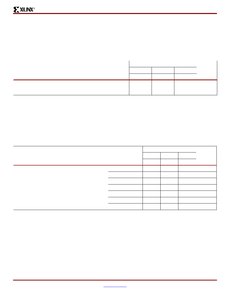
Global Clock Input to Output Delay for LVTTL, with DLL (Pin-to-Pin)(1)
Global Clock Input to Output Delay for LVTTL, without DLL (Pin-to-Pin)(1)
Symbol
Description
Speed Grade
Units
All
-7
-6
Min
Max
TICKOFDLL
LVTTL global clock input to output delay using
output flip-flop for LVTTL, 12 mA, fast slew rate,
with DLL.
1.0
3.1
ns
Notes:
1.
Listed above are representative values where one global clock input drives one vertical clock line in each accessible column, and
where all accessible IOB and CLB flip-flops are clocked by the global clock net.
2.
Output timing is measured at 1.4V with 35 pF external capacitive load for LVTTL. The 35 pF load does not apply to the Min values.
For other I/O standards and different loads, see the tables Constants for Calculating TIOOP and Delay Measurement Methodology,
3.
DLL output jitter is already included in the timing calculation.
4.
For data output with different standards, adjust delays with the values shown in IOB Output Delay Adjustments for Different
Standards(1), page 40. For a global clock input with standards other than LVTTL, adjust delays with values from the I/O Standard
Symbol
Description
Device
Speed Grade
Units
All
-7
-6
Min
Max
TICKOF
LVTTL global clock input to output
delay using output flip-flop for
LVTTL, 12 mA, fast slew rate,
without DLL.
XC2S50E
1.5
4.4
4.6
ns
XC2S100E
1.5
4.4
4.6
ns
XC2S150E
1.5
4.5
4.7
ns
XC2S200E
1.5
4.5
4.7
ns
XC2S300E
1.5
4.5
4.7
ns
XC2S400E
1.5
4.6
4.8
ns
XC2S600E
1.6
4.7
4.9
ns
Notes:
1.
Listed above are representative values where one global clock input drives one vertical clock line in each accessible column, and
where all accessible IOB and CLB flip-flops are clocked by the global clock net.
2.
Output timing is measured at 1.4V with 35 pF external capacitive load for LVTTL. The 35 pF load does not apply to the Min values.
For other I/O standards and different loads, see the tables Constants for Calculating TIOOP and Delay Measurement Methodology,
3.
For data output with different standards, adjust delays with the values shown in IOB Output Delay Adjustments for Different
Standards(1), page 40. For a global clock input with standards other than LVTTL, adjust delays with values from the I/O Standard
相關(guān)PDF資料 |
PDF描述 |
|---|---|
| XA3S250E-4PQG208I | IC FPGA SPARTAN-3E 250K 208-PQFP |
| XA3S400-4PQG208I | IC FPGA SPARTAN-3 400K 208-PQFP |
| XC3S250E-4FT256I | IC FPGA SPARTAN 3E 256FTBGA |
| 93LC76BT-I/ST | IC EEPROM 8KBIT 512X16 8-TSSOP |
| 93LC76BT-I/MS | IC EEPROM 8KBIT 512X16 8-MSOP |
相關(guān)代理商/技術(shù)參數(shù) |
參數(shù)描述 |
|---|---|
| XC2S150E-6FTG256C | 制造商:XILINX 制造商全稱:XILINX 功能描述:Spartan-IIE FPGA |
| XC2S150E-6FTG256I | 制造商:XILINX 制造商全稱:XILINX 功能描述:Spartan-IIE FPGA |
| XC2S150E-6PQ208C | 制造商:XILINX 制造商全稱:XILINX 功能描述:Spartan-IIE 1.8V FPGA Family |
| XC2S150E-6PQ208C0818 | 制造商:Xilinx 功能描述: |
| XC2S150E-6PQ208I | 制造商:XILINX 制造商全稱:XILINX 功能描述:Spartan-IIE 1.8V FPGA Family |
發(fā)布緊急采購,3分鐘左右您將得到回復(fù)。