- 您現(xiàn)在的位置:買賣IC網 > PDF目錄383876 > T7689 (Lineage Power) 5.0 V T1 Quad Line Interface(5.0 V T1四線接口) PDF資料下載
參數(shù)資料
| 型號: | T7689 |
| 廠商: | Lineage Power |
| 英文描述: | 5.0 V T1 Quad Line Interface(5.0 V T1四線接口) |
| 中文描述: | 5.0V的T1四線接口(5.0V的T1四線接口) |
| 文件頁數(shù): | 19/38頁 |
| 文件大小: | 548K |
| 代理商: | T7689 |
第1頁第2頁第3頁第4頁第5頁第6頁第7頁第8頁第9頁第10頁第11頁第12頁第13頁第14頁第15頁第16頁第17頁第18頁當前第19頁第20頁第21頁第22頁第23頁第24頁第25頁第26頁第27頁第28頁第29頁第30頁第31頁第32頁第33頁第34頁第35頁第36頁第37頁第38頁
Data Sheet
May 1998
T7689 5.0 V T1 Quad Line Interface
19
Lucent Technologies Inc.
Microprocessor Interface
Overview
The device is equipped with a microprocessor interface
that can operate with most commercially available
microprocessors. Inputs MPMUX and MPMODE
(pins 20 and 21) are used to configure this interface
into one of four possible modes, as shown in Table 10.
The MPMUX setting selects either a multiplexed 8-bit
address/data bus (AD[7:0]) or a demultiplexed 4-bit
address bus (A[3:0]) and an 8-bit data bus (AD[7:0]).
The MPMODE setting selects the associated set of
control signals required to access a set of registers
within the device.
When the microprocessor interface is configured to
operate in the multiplexed address/data bus modes
(MPMUX = 1), the user has access to an internal chip
select function that allows the microprocessor to selec-
tively read/write a specific T7689 in a multiple T7689
environment (see the Internal Chip Select Function
section).
The microprocessor interface can operate at speeds up
to 16.384 MHz in interrupt-driven or polled
mode without requiring any wait-states. For micropro-
cessors operating at greater than 16.384 MHz, the
RDY_DTACK output is used to introduce wait-states in
the read/write cycles.
In the interrupt-driven mode, one or more device
alarms will assert the active-high INT output (pin 25)
once per alarm activation. After the microprocessor
reads the alarm status registers, the INT output will
deassert. In the polled mode, however, the micropro-
cessor monitors the various device alarm status by
periodically reading the alarm status registers without
the use of INT (pin 25). In both interrupt and polled
methods of alarm servicing, the status register will
clear on a microprocessor read cycle only when the
alarm condition within the signaling channel no longer
exists; otherwise, the register bit remains set.
Due to the device flexibility, there are no default power-
up or reset states, except for register 4. All read/write
registers must be written by the microprocessor on
system start-up to guarantee proper device functional-
ity.
Details concerning microprocessor interface configura-
tion modes, pinout definitions, clock specifications,
register bank architecture, and the I/O timing specifica-
tions and diagrams are described in the following sec-
tions.
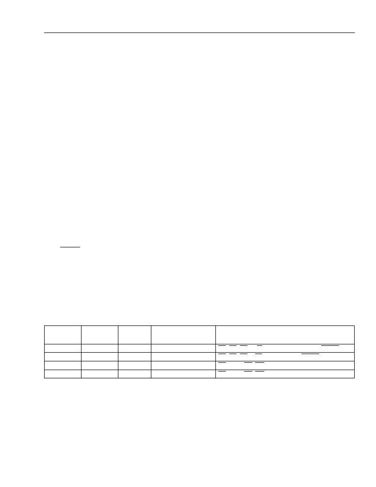
Microprocessor Configuration Modes
Table 10 highlights the four microprocessor modes controlled by the MPMUX and MPMODE inputs (pins 20 and
21).
Table 10. Microprocessor Configuration Modes
Mode
MPMODE
MPMUX
Address/Data Bus
Generic Control, Data, and
Output Pin Names
CS
,
AS
,
DS
, R/
W
, A[3:0], AD[7:0], INT,
DTACK
CS
,
AS
,
DS
, R
/W
, AD[7:0], INT,
DTACK
CS
, ALE,
RD
,
WR
, A[3:0], AD[7:0], INT, RDY
CS
, ALE,
RD
,
WR
, AD[7:0], INT, RDY
MODE1
MODE2
MODE3
MODE4
0
0
1
1
0
1
0
1
DEMUXed
MUXed
DEMUXed
MUXed
相關PDF資料 |
PDF描述 |
|---|---|
| T7690 | 5.0 V T1/E1 Quad Line Interface(5.0 V T1/E1 四線接口) |
| T7693 | 3.3 V T1/E1 Quad Line Interface( 3.3 V T1/E四線接口) |
| T7698 | Quad T1/E1 Line Interface and Octal T1/E1 Monitor(四T1/E1線接口和八T1/E1監(jiān)控器) |
| T7705A | SUPPLY-VOLTAGE SUPERVISORS |
| T8100A | H.100/H.110 Interface and Time-Slot Interchanger(H.100/H.110接口和干線時間段交換機) |
相關代理商/技術參數(shù) |
參數(shù)描述 |
|---|---|
| T-7689-FL | 制造商:Alcatel-Lucent 功能描述:DATACOM, PCM TRANSCEIVER, 100 Pin Plastic QFP |
| T-7689---FL-DB | 制造商:Rochester Electronics LLC 功能描述:- Bulk 制造商:LSI Corporation 功能描述: |
| T-7690-FL | 制造商:Alcatel-Lucent 功能描述:PCM TRANSCEIVER, Quad, CEPT PCM-30/E-1, 100 Pin, Plastic, QFP |
| T77 | 制造商:Thomas & Betts 功能描述:2-1/2"CONDUIT BODY,IRON,T,F-7 制造商:Cooper Crouse-Hinds 功能描述: 制造商:Thomas & Betts 功能描述:Fittings T-Fitting 2.5inch Non-Thread Iron |
| T7700 | 制造商:INTEL 制造商全稱:Intel Corporation 功能描述:Core2 Duo Processors and Core2 Extreme Processors for Platforms Based on Mobile 965 Express Chipset Family |
發(fā)布緊急采購,3分鐘左右您將得到回復。