- 您現(xiàn)在的位置:買(mǎi)賣(mài)IC網(wǎng) > PDF目錄383724 > ORT8850L Field-Programmable System Chip (FPSC) Eight-Channel x 850 Mbits/s Backplane Transceiver PDF資料下載
參數(shù)資料
| 型號(hào): | ORT8850L |
| 英文描述: | Field-Programmable System Chip (FPSC) Eight-Channel x 850 Mbits/s Backplane Transceiver |
| 中文描述: | 現(xiàn)場(chǎng)可編程系統(tǒng)芯片(促進(jìn)文化基金)8通道x 850 Mbits /秒背板收發(fā)器 |
| 文件頁(yè)數(shù): | 63/112頁(yè) |
| 文件大?。?/td> | 2417K |
| 代理商: | ORT8850L |
第1頁(yè)第2頁(yè)第3頁(yè)第4頁(yè)第5頁(yè)第6頁(yè)第7頁(yè)第8頁(yè)第9頁(yè)第10頁(yè)第11頁(yè)第12頁(yè)第13頁(yè)第14頁(yè)第15頁(yè)第16頁(yè)第17頁(yè)第18頁(yè)第19頁(yè)第20頁(yè)第21頁(yè)第22頁(yè)第23頁(yè)第24頁(yè)第25頁(yè)第26頁(yè)第27頁(yè)第28頁(yè)第29頁(yè)第30頁(yè)第31頁(yè)第32頁(yè)第33頁(yè)第34頁(yè)第35頁(yè)第36頁(yè)第37頁(yè)第38頁(yè)第39頁(yè)第40頁(yè)第41頁(yè)第42頁(yè)第43頁(yè)第44頁(yè)第45頁(yè)第46頁(yè)第47頁(yè)第48頁(yè)第49頁(yè)第50頁(yè)第51頁(yè)第52頁(yè)第53頁(yè)第54頁(yè)第55頁(yè)第56頁(yè)第57頁(yè)第58頁(yè)第59頁(yè)第60頁(yè)第61頁(yè)第62頁(yè)當(dāng)前第63頁(yè)第64頁(yè)第65頁(yè)第66頁(yè)第67頁(yè)第68頁(yè)第69頁(yè)第70頁(yè)第71頁(yè)第72頁(yè)第73頁(yè)第74頁(yè)第75頁(yè)第76頁(yè)第77頁(yè)第78頁(yè)第79頁(yè)第80頁(yè)第81頁(yè)第82頁(yè)第83頁(yè)第84頁(yè)第85頁(yè)第86頁(yè)第87頁(yè)第88頁(yè)第89頁(yè)第90頁(yè)第91頁(yè)第92頁(yè)第93頁(yè)第94頁(yè)第95頁(yè)第96頁(yè)第97頁(yè)第98頁(yè)第99頁(yè)第100頁(yè)第101頁(yè)第102頁(yè)第103頁(yè)第104頁(yè)第105頁(yè)第106頁(yè)第107頁(yè)第108頁(yè)第109頁(yè)第110頁(yè)第111頁(yè)第112頁(yè)
Agere Systems Inc.
63
Data Sheet
August 2001
Eight-Channel x 850 Mbits/s Backplane Transceiver
ORCA
ORT8850 FPSC
Pin Information
This section describes the pins and signals that perform FPGA-related functions. During configuration, the user-
programmable I/Os are 3-stated and pulled up with an internal resistor. If any FPGA function pin is not used (or not
bonded to package pin), it is also 3-stated and pulled up after configuration.
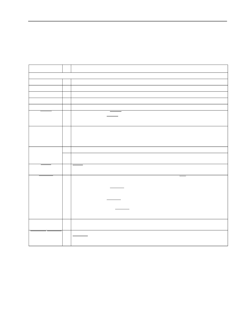
Table 29
.
FPGA Common-Function Pin Description
Symbol
I/O
Description
Dedicated Pins
V
DD
33
V
DD
15
V
DDIO
GND
PTEMP
RESET
—
3 V positive power supply.
—
1.5 V positive power supply for internal logic.
—
Positive power supply used by I/O banks.
—
Ground supply.
I
Temperature sensing diode pin. Dedicated input.
I
During configuration,
RESET
forces the restart of configuration and a pull-up is enabled.
After configuration,
RESET
can be used as a general FPGA input or as a direct input,
which causes all PLC latches/FFs to be asynchronously set/reset.
I
In the master and asynchronous peripheral modes, CCLK is an output which strobes con-
figuration data in. In the slave or readback after configuration, CCLK is input synchronous
with the data on DIN or D[7:0]. CCLK is an output for daisy-chain operation when the lead
device is in master, peripheral, or system bus modes.
I
As an input, a low level on DONE delays FPGA start up after configuration.*
O
As an active-high, open-drain output, a high level on this signal indicates that configura-
tion is complete. DONE has an optional pull-up resistor.
I
PRGM
is an active-low input that forces the restart of configuration and resets the bound-
ary scan circuitry. This pin always has an active pull-up.
I
This pin must be held high during device initialization until the
INIT
pin goes high. This pin
always has an active pull-up.
CCLK
O
DONE
PRGM
RD_CFG
During configuration,
RD_CFG
is an active-low input that activates the TS_ALL function
and 3-states all of the I/O.
After configuration,
RD_CFG
can be selected (via a bit stream option) to activate the
TS_ALL function as described above, or, if readback is enabled via a bit stream option, a
high-to-low transition on
RD_CFG
will initiate readback of the configuration data, including
PFU output states, starting with frame address 0.
RD_DATA/TDO is a dual-function pin. If used for readback, RD_DATA provides configu-
ration data out. If used in boundary scan, TDO is test data out.
During JTAG, slave, master, and asynchronous peripheral configuration assertion on this
CFG_IRQ
(active-low) indicates an error or errors for block RAM or FPSC initialization.
MPI
active-low interrupt request output.
RD_DATA/TDO
O
CFG_IRQ/MPI_IRQ
O
* The FPGA States of Operation section contains more information on how to control these signals during start up. The timing of DONE release
is controlled by one set of bit stream options, and the timing of the simultaneous release of all other configuration pins (and the activation of all
user I/Os) is controlled by a second set of options.
相關(guān)PDF資料 |
PDF描述 |
|---|---|
| OS1001 | Interface IC |
| OS1010 | Optoelectronic |
| OS1011 | SINGLE 1.8V, 200 KHZ OP, E TEMP, -40C to +125C, 8-PDIP, TUBE |
| OS1012 | 1.8V, 200kHz single low-cost, CMOS Op Amplifier on 120K Analog ROM process., -40C to +125C, 8-MSOP, T/R |
| OS1013 | 1.8V, 200kHz single low-cost, CMOS Op Amplifier on 120K Analog ROM proccess., -40C to +125C, 5-SOT-23, T/R |
相關(guān)代理商/技術(shù)參數(shù) |
參數(shù)描述 |
|---|---|
| ORT8850L-1BM680C | 功能描述:FPGA - 現(xiàn)場(chǎng)可編程門(mén)陣列 4992 LUT 278 I/O RoHS:否 制造商:Altera Corporation 系列:Cyclone V E 柵極數(shù)量: 邏輯塊數(shù)量:943 內(nèi)嵌式塊RAM - EBR:1956 kbit 輸入/輸出端數(shù)量:128 最大工作頻率:800 MHz 工作電源電壓:1.1 V 最大工作溫度:+ 70 C 安裝風(fēng)格:SMD/SMT 封裝 / 箱體:FBGA-256 |
| ORT8850L-1BM680I | 功能描述:FPGA - 現(xiàn)場(chǎng)可編程門(mén)陣列 4992 LUT 278 I/O RoHS:否 制造商:Altera Corporation 系列:Cyclone V E 柵極數(shù)量: 邏輯塊數(shù)量:943 內(nèi)嵌式塊RAM - EBR:1956 kbit 輸入/輸出端數(shù)量:128 最大工作頻率:800 MHz 工作電源電壓:1.1 V 最大工作溫度:+ 70 C 安裝風(fēng)格:SMD/SMT 封裝 / 箱體:FBGA-256 |
| ORT8850L-1BMN680C | 功能描述:FPGA - 現(xiàn)場(chǎng)可編程門(mén)陣列 4992 LUT 278 I/O RoHS:否 制造商:Altera Corporation 系列:Cyclone V E 柵極數(shù)量: 邏輯塊數(shù)量:943 內(nèi)嵌式塊RAM - EBR:1956 kbit 輸入/輸出端數(shù)量:128 最大工作頻率:800 MHz 工作電源電壓:1.1 V 最大工作溫度:+ 70 C 安裝風(fēng)格:SMD/SMT 封裝 / 箱體:FBGA-256 |
| ORT8850L-1BMN680I | 功能描述:FPGA - 現(xiàn)場(chǎng)可編程門(mén)陣列 4992 LUT 278 I/O RoHS:否 制造商:Altera Corporation 系列:Cyclone V E 柵極數(shù)量: 邏輯塊數(shù)量:943 內(nèi)嵌式塊RAM - EBR:1956 kbit 輸入/輸出端數(shù)量:128 最大工作頻率:800 MHz 工作電源電壓:1.1 V 最大工作溫度:+ 70 C 安裝風(fēng)格:SMD/SMT 封裝 / 箱體:FBGA-256 |
| ORT8850L-2BM680C | 功能描述:FPGA - 現(xiàn)場(chǎng)可編程門(mén)陣列 4992 LUT 278 I/O RoHS:否 制造商:Altera Corporation 系列:Cyclone V E 柵極數(shù)量: 邏輯塊數(shù)量:943 內(nèi)嵌式塊RAM - EBR:1956 kbit 輸入/輸出端數(shù)量:128 最大工作頻率:800 MHz 工作電源電壓:1.1 V 最大工作溫度:+ 70 C 安裝風(fēng)格:SMD/SMT 封裝 / 箱體:FBGA-256 |
發(fā)布緊急采購(gòu),3分鐘左右您將得到回復(fù)。