- 您現(xiàn)在的位置:買(mǎi)賣IC網(wǎng) > PDF目錄383724 > ORT8850L Field-Programmable System Chip (FPSC) Eight-Channel x 850 Mbits/s Backplane Transceiver PDF資料下載
參數(shù)資料
| 型號(hào): | ORT8850L |
| 英文描述: | Field-Programmable System Chip (FPSC) Eight-Channel x 850 Mbits/s Backplane Transceiver |
| 中文描述: | 現(xiàn)場(chǎng)可編程系統(tǒng)芯片(促進(jìn)文化基金)8通道x 850 Mbits /秒背板收發(fā)器 |
| 文件頁(yè)數(shù): | 22/112頁(yè) |
| 文件大?。?/td> | 2417K |
| 代理商: | ORT8850L |
第1頁(yè)第2頁(yè)第3頁(yè)第4頁(yè)第5頁(yè)第6頁(yè)第7頁(yè)第8頁(yè)第9頁(yè)第10頁(yè)第11頁(yè)第12頁(yè)第13頁(yè)第14頁(yè)第15頁(yè)第16頁(yè)第17頁(yè)第18頁(yè)第19頁(yè)第20頁(yè)第21頁(yè)當(dāng)前第22頁(yè)第23頁(yè)第24頁(yè)第25頁(yè)第26頁(yè)第27頁(yè)第28頁(yè)第29頁(yè)第30頁(yè)第31頁(yè)第32頁(yè)第33頁(yè)第34頁(yè)第35頁(yè)第36頁(yè)第37頁(yè)第38頁(yè)第39頁(yè)第40頁(yè)第41頁(yè)第42頁(yè)第43頁(yè)第44頁(yè)第45頁(yè)第46頁(yè)第47頁(yè)第48頁(yè)第49頁(yè)第50頁(yè)第51頁(yè)第52頁(yè)第53頁(yè)第54頁(yè)第55頁(yè)第56頁(yè)第57頁(yè)第58頁(yè)第59頁(yè)第60頁(yè)第61頁(yè)第62頁(yè)第63頁(yè)第64頁(yè)第65頁(yè)第66頁(yè)第67頁(yè)第68頁(yè)第69頁(yè)第70頁(yè)第71頁(yè)第72頁(yè)第73頁(yè)第74頁(yè)第75頁(yè)第76頁(yè)第77頁(yè)第78頁(yè)第79頁(yè)第80頁(yè)第81頁(yè)第82頁(yè)第83頁(yè)第84頁(yè)第85頁(yè)第86頁(yè)第87頁(yè)第88頁(yè)第89頁(yè)第90頁(yè)第91頁(yè)第92頁(yè)第93頁(yè)第94頁(yè)第95頁(yè)第96頁(yè)第97頁(yè)第98頁(yè)第99頁(yè)第100頁(yè)第101頁(yè)第102頁(yè)第103頁(yè)第104頁(yè)第105頁(yè)第106頁(yè)第107頁(yè)第108頁(yè)第109頁(yè)第110頁(yè)第111頁(yè)第112頁(yè)
22
Agere Systems Inc.
Data Sheet
August 2001
Eight-Channel x 850 Mbits/s Backplane Transceiver
ORCA
ORT8850 FPSC
Backplane Transceiver Core Detailed Description
(continued)
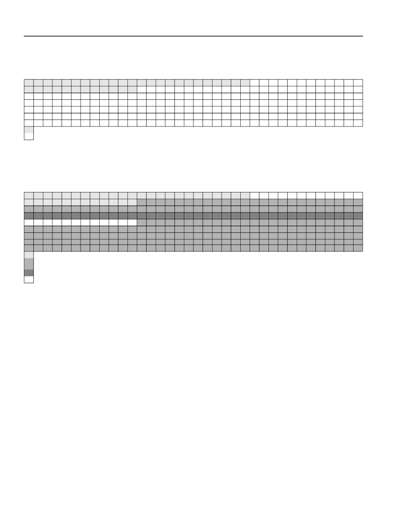
Table 2. Transmitter TOH on LVDS Output (Transparent Mode)
In the TOH insert mode of operation, TOH bytes on LVDS output are shown in Table 3. This also shows the order
in which data is transferred to the serial TOH interface, starting with the most significant bit of the first A1 byte. The
first bit of the first byte is replaced by an even parity check bit over all TOH bytes from the previous TOH frame.
Table 3. Transmitter TOH on LVDS Output (TOH Insert Mode)
A1/A2 Frame Insert and Testing
The A1 and A2 bytes provide a special framing pattern that indicates where a STS-1 begins in a bit stream. All
12 A1 bytes of each STS-12 are set to 0xF6, and all 12 A2 bytes of the STS-12 are set to 0x28 when not overrid-
den with an user-specified value for testing. The latency from the transmission of the first bit of the A1 byte at the
device output pins from the transmit frame pulse (SYS_FP) at the FPGA to embedded core input is between five to
seven cycles of fpga_sysclk.
A1/A2 testing (corruption) is controlled per stream by the A1/A2 error insert register. When A1/A2 corruption detec-
tion is set for a particular stream, the A1/A2 values in the corrupted A1/A2 value registers are sent for the number
of frames defined in the corrupted A1/A2 frame count register. When the corrupted A1/A2 frame count register is
set to zero, A1/A2 corruption will continue until the A1/A2 error insert register is cleared. This also allows alternate
values to be set for A1 and A2 during normal operation. For the ORT8850, it is optionally possible to not insert A1
and A2.
On a per-device basis, the A1 and A2 byte values are set, as well as the number of frames of corruption. Then, to
insert the specified A1/A2 values, each channel has an enable register. When the enable register is set, the A1/A2
values are corrupted for the number specified in the number of frames to corrupt. To insert errors again, the per-
channel fault insert register must be cleared, and set again. Only the last A1 and the first A2 are corrupted.
A1
B1
A1
0
A1
0
A1
0
A1
0
A1
0
A1
0
A1
0
A1
0
A1
0
A1
0
A1
0
A2
A2
A2
A2
A2
A2
A2
A2
A2
A2
A2
A2
Regenerated bytes.
Transparent bytes from parallel input port.
A1
B1
D1
H1
A1
0
D1
H1
A1
0
D1
H1
A1
0
D1
H1
A1
0
D1
H1
A1
0
D1
H1
A1
0
D1
H1
A1
0
D1
H1
A1
0
D1
H1
A1
0
D1
H1
A1
0
D1
H1
A1
0
D1
H1
A2
E1
D2
H2
K1
D5
D8
A2
E1
D2
H2
K1
D5
D8
A2
E1
D2
H2
K1
D5
D8
A2
E1
D2
H2
K1
D5
D8
A2
E1
D2
H2
K1
D5
D8
A2
E1
D2
H2
K1
D5
D8
A2
E1
D2
H2
K1
D5
D8
A2
E1
D2
H2
K1
D5
D8
A2
E1
D2
H2
K1
D5
D8
A2
E1
D2
H2
K1
D5
D8
A2
E1
D2
H2
K1
D5
D8
A2
E1
D2
H2
K1
D5
D8
F1
D3
H3
K2
D6
D9
F1
D3
H3
K2
D6
D9
F1
D3
H3
K2
D6
D9
F1
D3
H3
K2
D6
D9
F1
D3
H3
K2
D6
D9
F1
D3
H3
K2
D6
D9
F1
D3
H3
K2
D6
D9
F1
D3
H3
K2
D6
D9
F1
D3
H3
K2
D6
D9
F1
D3
H3
K2
D6
D9
F1
D3
H3
K2
D6
D9
F1
D3
H3
K2
D6
D9
D4
D7
D4
D7
D4
D7
D4
D7
D4
D7
D4
D7
D4
D7
D4
D7
D4
D7
D4
D7
D4
D7
D4
D7
D10
S1
D10
S1
Regenerated bytes.
Inserted or transparent bytes. Blocks of 12 STS-1 bytes are controlled as a whole. There are 15 controls/channel: K1/K2, S1/M0, E1/F1/E2, D1, D2, D3, D4, D5, D6, D7, D8, D9, D10,
D11, D12.
D10
S1
D10
S1
D10
S1
D10
S1
D10
S1
D10
S1
D10
S1
D10
S1
D10
S1
D10
S1
D11
D11
D11
D11
D11
D11
D11
D11
D11
D11
D11
D11
D12
E2
D12
E2
D12
E2
D12
E2
D12
E2
D12
E2
D12
E2
D12
E2
D12
E2
D12
E2
D12
E2
D12
E2
M0
M0
M0
M0
M0
M0
M0
M0
M0
M0
M0
M0
Transparent bytes (from parallel input port).
Inserted bytes from TOH serial input port.
相關(guān)PDF資料 |
PDF描述 |
|---|---|
| OS1001 | Interface IC |
| OS1010 | Optoelectronic |
| OS1011 | SINGLE 1.8V, 200 KHZ OP, E TEMP, -40C to +125C, 8-PDIP, TUBE |
| OS1012 | 1.8V, 200kHz single low-cost, CMOS Op Amplifier on 120K Analog ROM process., -40C to +125C, 8-MSOP, T/R |
| OS1013 | 1.8V, 200kHz single low-cost, CMOS Op Amplifier on 120K Analog ROM proccess., -40C to +125C, 5-SOT-23, T/R |
相關(guān)代理商/技術(shù)參數(shù) |
參數(shù)描述 |
|---|---|
| ORT8850L-1BM680C | 功能描述:FPGA - 現(xiàn)場(chǎng)可編程門(mén)陣列 4992 LUT 278 I/O RoHS:否 制造商:Altera Corporation 系列:Cyclone V E 柵極數(shù)量: 邏輯塊數(shù)量:943 內(nèi)嵌式塊RAM - EBR:1956 kbit 輸入/輸出端數(shù)量:128 最大工作頻率:800 MHz 工作電源電壓:1.1 V 最大工作溫度:+ 70 C 安裝風(fēng)格:SMD/SMT 封裝 / 箱體:FBGA-256 |
| ORT8850L-1BM680I | 功能描述:FPGA - 現(xiàn)場(chǎng)可編程門(mén)陣列 4992 LUT 278 I/O RoHS:否 制造商:Altera Corporation 系列:Cyclone V E 柵極數(shù)量: 邏輯塊數(shù)量:943 內(nèi)嵌式塊RAM - EBR:1956 kbit 輸入/輸出端數(shù)量:128 最大工作頻率:800 MHz 工作電源電壓:1.1 V 最大工作溫度:+ 70 C 安裝風(fēng)格:SMD/SMT 封裝 / 箱體:FBGA-256 |
| ORT8850L-1BMN680C | 功能描述:FPGA - 現(xiàn)場(chǎng)可編程門(mén)陣列 4992 LUT 278 I/O RoHS:否 制造商:Altera Corporation 系列:Cyclone V E 柵極數(shù)量: 邏輯塊數(shù)量:943 內(nèi)嵌式塊RAM - EBR:1956 kbit 輸入/輸出端數(shù)量:128 最大工作頻率:800 MHz 工作電源電壓:1.1 V 最大工作溫度:+ 70 C 安裝風(fēng)格:SMD/SMT 封裝 / 箱體:FBGA-256 |
| ORT8850L-1BMN680I | 功能描述:FPGA - 現(xiàn)場(chǎng)可編程門(mén)陣列 4992 LUT 278 I/O RoHS:否 制造商:Altera Corporation 系列:Cyclone V E 柵極數(shù)量: 邏輯塊數(shù)量:943 內(nèi)嵌式塊RAM - EBR:1956 kbit 輸入/輸出端數(shù)量:128 最大工作頻率:800 MHz 工作電源電壓:1.1 V 最大工作溫度:+ 70 C 安裝風(fēng)格:SMD/SMT 封裝 / 箱體:FBGA-256 |
| ORT8850L-2BM680C | 功能描述:FPGA - 現(xiàn)場(chǎng)可編程門(mén)陣列 4992 LUT 278 I/O RoHS:否 制造商:Altera Corporation 系列:Cyclone V E 柵極數(shù)量: 邏輯塊數(shù)量:943 內(nèi)嵌式塊RAM - EBR:1956 kbit 輸入/輸出端數(shù)量:128 最大工作頻率:800 MHz 工作電源電壓:1.1 V 最大工作溫度:+ 70 C 安裝風(fēng)格:SMD/SMT 封裝 / 箱體:FBGA-256 |
發(fā)布緊急采購(gòu),3分鐘左右您將得到回復(fù)。