- 您現(xiàn)在的位置:買賣IC網(wǎng) > PDF目錄383724 > ORT8850H Field-Programmable System Chip (FPSC) Eight-Channel x 850 Mbits/s Backplane Transceiver PDF資料下載
參數(shù)資料
| 型號: | ORT8850H |
| 英文描述: | Field-Programmable System Chip (FPSC) Eight-Channel x 850 Mbits/s Backplane Transceiver |
| 中文描述: | 現(xiàn)場可編程系統(tǒng)芯片(促進(jìn)文化基金)8通道x 850 Mbits /秒背板收發(fā)器 |
| 文件頁數(shù): | 47/112頁 |
| 文件大小: | 2417K |
| 代理商: | ORT8850H |
第1頁第2頁第3頁第4頁第5頁第6頁第7頁第8頁第9頁第10頁第11頁第12頁第13頁第14頁第15頁第16頁第17頁第18頁第19頁第20頁第21頁第22頁第23頁第24頁第25頁第26頁第27頁第28頁第29頁第30頁第31頁第32頁第33頁第34頁第35頁第36頁第37頁第38頁第39頁第40頁第41頁第42頁第43頁第44頁第45頁第46頁當(dāng)前第47頁第48頁第49頁第50頁第51頁第52頁第53頁第54頁第55頁第56頁第57頁第58頁第59頁第60頁第61頁第62頁第63頁第64頁第65頁第66頁第67頁第68頁第69頁第70頁第71頁第72頁第73頁第74頁第75頁第76頁第77頁第78頁第79頁第80頁第81頁第82頁第83頁第84頁第85頁第86頁第87頁第88頁第89頁第90頁第91頁第92頁第93頁第94頁第95頁第96頁第97頁第98頁第99頁第100頁第101頁第102頁第103頁第104頁第105頁第106頁第107頁第108頁第109頁第110頁第111頁第112頁
Agere Systems Inc.
47
Data Sheet
August 2001
Eight-Channel x 850 Mbits/s Backplane Transceiver
ORCA
ORT8850 FPSC
Memory Map
(continued)
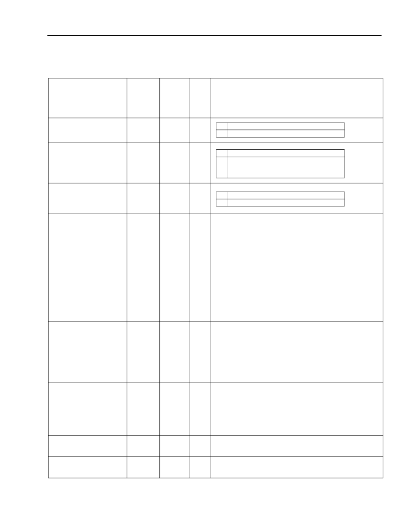
Table 12. Memory Map Descriptions
(continued)
Bit/Register Name(S)
Bit/
Register
Location
(Hex)
Register
Type
Reset
Value
(Hex)
Description
input/output parallel bus
parity control
0C [5]
creg
1
scrambler/descrambler
control
0C [6]
creg
1
transmit B1 error insert
mask [0:7]
0F [0:7]
creg
00
ch 1 int
ch 2 int
ch 3 int
ch 4 int
per device int
enable/mask register for
ch 1-4 + device[4:0]
ch 5 int
ch 6 int
ch 7 int
ch 8 int
enable/mask register for
ch 5-8 [0:3]
10 [0]
10 [1]
10 [2]
10 [3]
10 [4]
11 [0:4]
14 [0]
14 [1]
14 [2]
14 [3]
15 [0:3]
isreg
isreg
isreg
isreg
isreg
iereg
isreg
isreg
isreg
isreg
iereg
0
0
0
0
0
0
0
0
0
0
0
Consolidation interrupts. 1 = interrupt, 0 = no interrupt.
frame offset error flag
write to locked register
error flag
enable/mask register [0:1]
12 [0]
12 [1]
13 [0:1]
iareg
iareg
iereg
0
0
0
If in the receive direction the phase offset between any two
channels exceeds 17 bytes, then a frame offset error event
will be issued. This condition is continuously monitored.
If the core memory map has not been unlocked (by writing
to the lock registers), and any address other than the lock-
reg registers or scratch pad register is written to, then a
“
write to locked register
”
event will be generated.
STM A mode control
STM B mode control
16 [2:3]
16 [0:1]
creg
creg
0
0
00 - Quad STS-12 or STS-48.
01 - Quad STS-3.
10 - Quad STS-1.
00 - Quad STS-12 or STS-48.
01 - Quad STS-3.
10 - Quad STS-1.
individual alignment
resync register
17 [0:7]
creg
0
Write 1 to resync stream.
group alignment resync
register
18 [0:7]
creg
0
Write 1 to resync selected grouping.
0
Even parity.
1
Odd parity.
0
no rx direction, descramble / tx direction scramble.
1
In rx direction, descramble channel after SONET frame recov-
ery.
In tx direction, scramble data just before parallel-to-serial con-
version.
0
No error insertion.
1
Invert corresponding bit in B1 byte.
相關(guān)PDF資料 |
PDF描述 |
|---|---|
| ORT8850L | Field-Programmable System Chip (FPSC) Eight-Channel x 850 Mbits/s Backplane Transceiver |
| OS1001 | Interface IC |
| OS1010 | Optoelectronic |
| OS1011 | SINGLE 1.8V, 200 KHZ OP, E TEMP, -40C to +125C, 8-PDIP, TUBE |
| OS1012 | 1.8V, 200kHz single low-cost, CMOS Op Amplifier on 120K Analog ROM process., -40C to +125C, 8-MSOP, T/R |
相關(guān)代理商/技術(shù)參數(shù) |
參數(shù)描述 |
|---|---|
| ORT8850H-1BM680C | 功能描述:FPGA - 現(xiàn)場可編程門陣列 16192 LUT 297 I/O RoHS:否 制造商:Altera Corporation 系列:Cyclone V E 柵極數(shù)量: 邏輯塊數(shù)量:943 內(nèi)嵌式塊RAM - EBR:1956 kbit 輸入/輸出端數(shù)量:128 最大工作頻率:800 MHz 工作電源電壓:1.1 V 最大工作溫度:+ 70 C 安裝風(fēng)格:SMD/SMT 封裝 / 箱體:FBGA-256 |
| ORT8850H-1BM680I | 功能描述:FPGA - 現(xiàn)場可編程門陣列 16192 LUT 297 I/O RoHS:否 制造商:Altera Corporation 系列:Cyclone V E 柵極數(shù)量: 邏輯塊數(shù)量:943 內(nèi)嵌式塊RAM - EBR:1956 kbit 輸入/輸出端數(shù)量:128 最大工作頻率:800 MHz 工作電源電壓:1.1 V 最大工作溫度:+ 70 C 安裝風(fēng)格:SMD/SMT 封裝 / 箱體:FBGA-256 |
| ORT8850H-1BMN680C | 功能描述:FPGA - 現(xiàn)場可編程門陣列 16192 LUT 297 I/O RoHS:否 制造商:Altera Corporation 系列:Cyclone V E 柵極數(shù)量: 邏輯塊數(shù)量:943 內(nèi)嵌式塊RAM - EBR:1956 kbit 輸入/輸出端數(shù)量:128 最大工作頻率:800 MHz 工作電源電壓:1.1 V 最大工作溫度:+ 70 C 安裝風(fēng)格:SMD/SMT 封裝 / 箱體:FBGA-256 |
| ORT8850H-1BMN680I | 功能描述:FPGA - 現(xiàn)場可編程門陣列 16192 LUT 297 I/O RoHS:否 制造商:Altera Corporation 系列:Cyclone V E 柵極數(shù)量: 邏輯塊數(shù)量:943 內(nèi)嵌式塊RAM - EBR:1956 kbit 輸入/輸出端數(shù)量:128 最大工作頻率:800 MHz 工作電源電壓:1.1 V 最大工作溫度:+ 70 C 安裝風(fēng)格:SMD/SMT 封裝 / 箱體:FBGA-256 |
| ORT8850H-2BM680C | 功能描述:FPGA - 現(xiàn)場可編程門陣列 16192 LUT 297 I/O RoHS:否 制造商:Altera Corporation 系列:Cyclone V E 柵極數(shù)量: 邏輯塊數(shù)量:943 內(nèi)嵌式塊RAM - EBR:1956 kbit 輸入/輸出端數(shù)量:128 最大工作頻率:800 MHz 工作電源電壓:1.1 V 最大工作溫度:+ 70 C 安裝風(fēng)格:SMD/SMT 封裝 / 箱體:FBGA-256 |
發(fā)布緊急采購,3分鐘左右您將得到回復(fù)。