- 您現(xiàn)在的位置:買賣IC網(wǎng) > PDF目錄383724 > ORT8850H Field-Programmable System Chip (FPSC) Eight-Channel x 850 Mbits/s Backplane Transceiver PDF資料下載
參數(shù)資料
| 型號(hào): | ORT8850H |
| 英文描述: | Field-Programmable System Chip (FPSC) Eight-Channel x 850 Mbits/s Backplane Transceiver |
| 中文描述: | 現(xiàn)場(chǎng)可編程系統(tǒng)芯片(促進(jìn)文化基金)8通道x 850 Mbits /秒背板收發(fā)器 |
| 文件頁數(shù): | 20/112頁 |
| 文件大小: | 2417K |
| 代理商: | ORT8850H |
第1頁第2頁第3頁第4頁第5頁第6頁第7頁第8頁第9頁第10頁第11頁第12頁第13頁第14頁第15頁第16頁第17頁第18頁第19頁當(dāng)前第20頁第21頁第22頁第23頁第24頁第25頁第26頁第27頁第28頁第29頁第30頁第31頁第32頁第33頁第34頁第35頁第36頁第37頁第38頁第39頁第40頁第41頁第42頁第43頁第44頁第45頁第46頁第47頁第48頁第49頁第50頁第51頁第52頁第53頁第54頁第55頁第56頁第57頁第58頁第59頁第60頁第61頁第62頁第63頁第64頁第65頁第66頁第67頁第68頁第69頁第70頁第71頁第72頁第73頁第74頁第75頁第76頁第77頁第78頁第79頁第80頁第81頁第82頁第83頁第84頁第85頁第86頁第87頁第88頁第89頁第90頁第91頁第92頁第93頁第94頁第95頁第96頁第97頁第98頁第99頁第100頁第101頁第102頁第103頁第104頁第105頁第106頁第107頁第108頁第109頁第110頁第111頁第112頁
20
Agere Systems Inc.
Data Sheet
August 2001
Eight-Channel x 850 Mbits/s Backplane Transceiver
ORCA
ORT8850 FPSC
Backplane Transceiver Core Detailed
Description
(continued)
STM Transmitter (FPGA
→
Backplane)
The synchronous transport module (STM) portion of
the embedded core consists of two slices: STM A and
B.
Each STM slice has four STS-12 transmit channels,
which can be treated as a single STS-48 channel. In
general, the transmitter circuit receives four byte-wide
77.76 MHz data from the FPGA, which nominally rep-
resents four STS-12 streams (A, B, C, and D). This
data is synchronized to the system (reference) clock,
and an 8 kHz
system frame pulse from the FPGA logic.
Transport overhead bytes are then optionally inserted
into these streams, and the streams are forwarded to
the HSI. All byte timing pulses required to isolate indi-
vidual overhead bytes (e.g., A1, A2, B1, D1
—
D3, etc.)
are generated internally based on the system frame
pulse (SYS_FP) received from the FPGA logic. All
streams operate byte-wide at 77.76 MHz in all modes.
The TOH processor operates from 25 MHz to
77.76 MHz and supports the following TOH signals: A1
and A2 insertion and optional corruption; H1, H2, and
H3 pass transparently; BIP-8 parity calculation (after
scrambling) and B1 byte insertion and optional corrup-
tion (before scrambling); optional K1 and K2 insert;
optional S1/M0 insert; optional E1/F1/E2 insert;
optional section data communication channel (DCC,
D1
—
D3) and line data communication channel (DCC,
D4
—
D12) insertion (for intercard communications
channel); scrambling of outgoing data stream with
optional scrambler disabling; and optional stream dis-
abling. All streams operate byte-wide at 77.76 MHz
(622 Mbits/s) or 106.25 MHz (850 Mbits/s) in all modes.
When the ORT8850 is used in nonnetworking applica-
tions as a generic high-speed backplane data mover,
the TOH serial ports are unused or can be used for
slow-speed, off-channel communication between
devices. An optional transparent mode is available
where only the twelve A1 and twelve A2 bytes are used
for frame alignment and synchronization.
Data received on the parallel bus is optionally scram-
bled and transferred to LVDS outputs.
Byte Ordering Information
The STM macro slice (i.e., A, B) supports quad STS-
12, quad STS-3, and quad STS-1 modes of operation
on the input/output ports. STS-48 is also supported, but
it must be received in the quad STS-12 format. When
operating in quad STS-12 mode, each of the indepen-
dent byte streams carries an entire STS-12 within it.
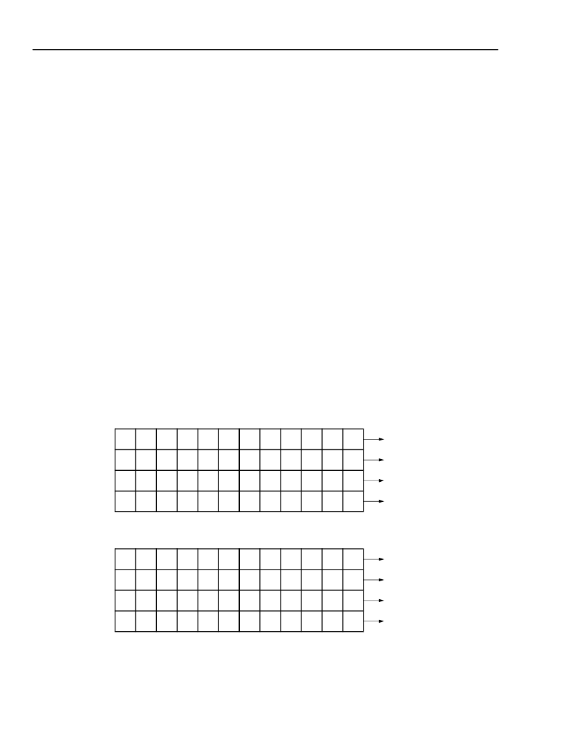
Figure 5 reveals the byte ordering of the individual
STS-12 streams and for STS-48 operation. Note that
the recovered data will always continue to be in the
same order as transmitted.
5-8574 (F)
Figure 5. Byte Ordering of Input/Output Interface in STS-12 Mode
12
24
36
48
9
21
33
45
6
18
30
42
3
15
27
39
11
23
35
47
8
20
32
44
5
17
29
41
2
14
26
38
10
22
34
46
7
19
31
43
4
16
28
40
1
13
25
37
1, 12
2, 12
3, 12
4, 12
1, 9
2, 9
3, 9
4, 9
1, 6
2, 6
3, 6
4, 6
1, 3
2, 3
3, 3
4, 3
1, 11
2, 11
3, 11
4, 11
1, 8
2, 8
3, 8
4, 8
1, 5
2, 5
3, 5
4, 5
1, 2
2, 2
3, 2
4, 2
1, 10
2, 10
3, 10
4, 10
1, 7
2, 7
3, 7
4, 7
1, 4
2, 4
3, 4
4, 4
1, 1
2, 1
3, 1
4, 1
STS-12 A
STS-12 B
STS-12 C
STS-12 D
STS-12 A
STS-12 B
STS-12 C
STS-12 D
STS-48 IN QUAD STS-12 FORMAT
QUAD STS-12
相關(guān)PDF資料 |
PDF描述 |
|---|---|
| ORT8850L | Field-Programmable System Chip (FPSC) Eight-Channel x 850 Mbits/s Backplane Transceiver |
| OS1001 | Interface IC |
| OS1010 | Optoelectronic |
| OS1011 | SINGLE 1.8V, 200 KHZ OP, E TEMP, -40C to +125C, 8-PDIP, TUBE |
| OS1012 | 1.8V, 200kHz single low-cost, CMOS Op Amplifier on 120K Analog ROM process., -40C to +125C, 8-MSOP, T/R |
相關(guān)代理商/技術(shù)參數(shù) |
參數(shù)描述 |
|---|---|
| ORT8850H-1BM680C | 功能描述:FPGA - 現(xiàn)場(chǎng)可編程門陣列 16192 LUT 297 I/O RoHS:否 制造商:Altera Corporation 系列:Cyclone V E 柵極數(shù)量: 邏輯塊數(shù)量:943 內(nèi)嵌式塊RAM - EBR:1956 kbit 輸入/輸出端數(shù)量:128 最大工作頻率:800 MHz 工作電源電壓:1.1 V 最大工作溫度:+ 70 C 安裝風(fēng)格:SMD/SMT 封裝 / 箱體:FBGA-256 |
| ORT8850H-1BM680I | 功能描述:FPGA - 現(xiàn)場(chǎng)可編程門陣列 16192 LUT 297 I/O RoHS:否 制造商:Altera Corporation 系列:Cyclone V E 柵極數(shù)量: 邏輯塊數(shù)量:943 內(nèi)嵌式塊RAM - EBR:1956 kbit 輸入/輸出端數(shù)量:128 最大工作頻率:800 MHz 工作電源電壓:1.1 V 最大工作溫度:+ 70 C 安裝風(fēng)格:SMD/SMT 封裝 / 箱體:FBGA-256 |
| ORT8850H-1BMN680C | 功能描述:FPGA - 現(xiàn)場(chǎng)可編程門陣列 16192 LUT 297 I/O RoHS:否 制造商:Altera Corporation 系列:Cyclone V E 柵極數(shù)量: 邏輯塊數(shù)量:943 內(nèi)嵌式塊RAM - EBR:1956 kbit 輸入/輸出端數(shù)量:128 最大工作頻率:800 MHz 工作電源電壓:1.1 V 最大工作溫度:+ 70 C 安裝風(fēng)格:SMD/SMT 封裝 / 箱體:FBGA-256 |
| ORT8850H-1BMN680I | 功能描述:FPGA - 現(xiàn)場(chǎng)可編程門陣列 16192 LUT 297 I/O RoHS:否 制造商:Altera Corporation 系列:Cyclone V E 柵極數(shù)量: 邏輯塊數(shù)量:943 內(nèi)嵌式塊RAM - EBR:1956 kbit 輸入/輸出端數(shù)量:128 最大工作頻率:800 MHz 工作電源電壓:1.1 V 最大工作溫度:+ 70 C 安裝風(fēng)格:SMD/SMT 封裝 / 箱體:FBGA-256 |
| ORT8850H-2BM680C | 功能描述:FPGA - 現(xiàn)場(chǎng)可編程門陣列 16192 LUT 297 I/O RoHS:否 制造商:Altera Corporation 系列:Cyclone V E 柵極數(shù)量: 邏輯塊數(shù)量:943 內(nèi)嵌式塊RAM - EBR:1956 kbit 輸入/輸出端數(shù)量:128 最大工作頻率:800 MHz 工作電源電壓:1.1 V 最大工作溫度:+ 70 C 安裝風(fēng)格:SMD/SMT 封裝 / 箱體:FBGA-256 |
發(fā)布緊急采購,3分鐘左右您將得到回復(fù)。