- 您現(xiàn)在的位置:買賣IC網(wǎng) > PDF目錄370849 > M37754S4CGP (Mitsubishi Electric Corporation) SINGLE-CHIP 16BIT CMOS MICROCOMPUTER PDF資料下載
參數(shù)資料
| 型號: | M37754S4CGP |
| 廠商: | Mitsubishi Electric Corporation |
| 英文描述: | SINGLE-CHIP 16BIT CMOS MICROCOMPUTER |
| 中文描述: | 單芯片16位微機(jī)的CMOS |
| 文件頁數(shù): | 62/114頁 |
| 文件大?。?/td> | 1116K |
| 代理商: | M37754S4CGP |
第1頁第2頁第3頁第4頁第5頁第6頁第7頁第8頁第9頁第10頁第11頁第12頁第13頁第14頁第15頁第16頁第17頁第18頁第19頁第20頁第21頁第22頁第23頁第24頁第25頁第26頁第27頁第28頁第29頁第30頁第31頁第32頁第33頁第34頁第35頁第36頁第37頁第38頁第39頁第40頁第41頁第42頁第43頁第44頁第45頁第46頁第47頁第48頁第49頁第50頁第51頁第52頁第53頁第54頁第55頁第56頁第57頁第58頁第59頁第60頁第61頁當(dāng)前第62頁第63頁第64頁第65頁第66頁第67頁第68頁第69頁第70頁第71頁第72頁第73頁第74頁第75頁第76頁第77頁第78頁第79頁第80頁第81頁第82頁第83頁第84頁第85頁第86頁第87頁第88頁第89頁第90頁第91頁第92頁第93頁第94頁第95頁第96頁第97頁第98頁第99頁第100頁第101頁第102頁第103頁第104頁第105頁第106頁第107頁第108頁第109頁第110頁第111頁第112頁第113頁第114頁
62
PRELIMINARY
Notice: This is not a final specification.
Some parametric limits are subject to change.
MITSUBISHI MICROCOMPUTERS
M37754M8C-XXXGP, M37754M8C-XXXHP
M37754S4CGP, M37754S4CHP
SINGLE-CHIP 16-BIT CMOS MICROCOMPUTER
RESET CIRCUIT
Reset is released when the RESET pin is returned to “H” level after
holding it at “L” level while the supply voltage is at 5V ±10%. As the
result, program execution starts at the address formed by setting the
address A
23
–A
16
to 00
16
, A
15
–A
8
to the contents of address FFFF
16
,
and A
7
–A
0
to the contents of address FFFE
16
.
Figure 76 shows the status of the internal registers during reset.
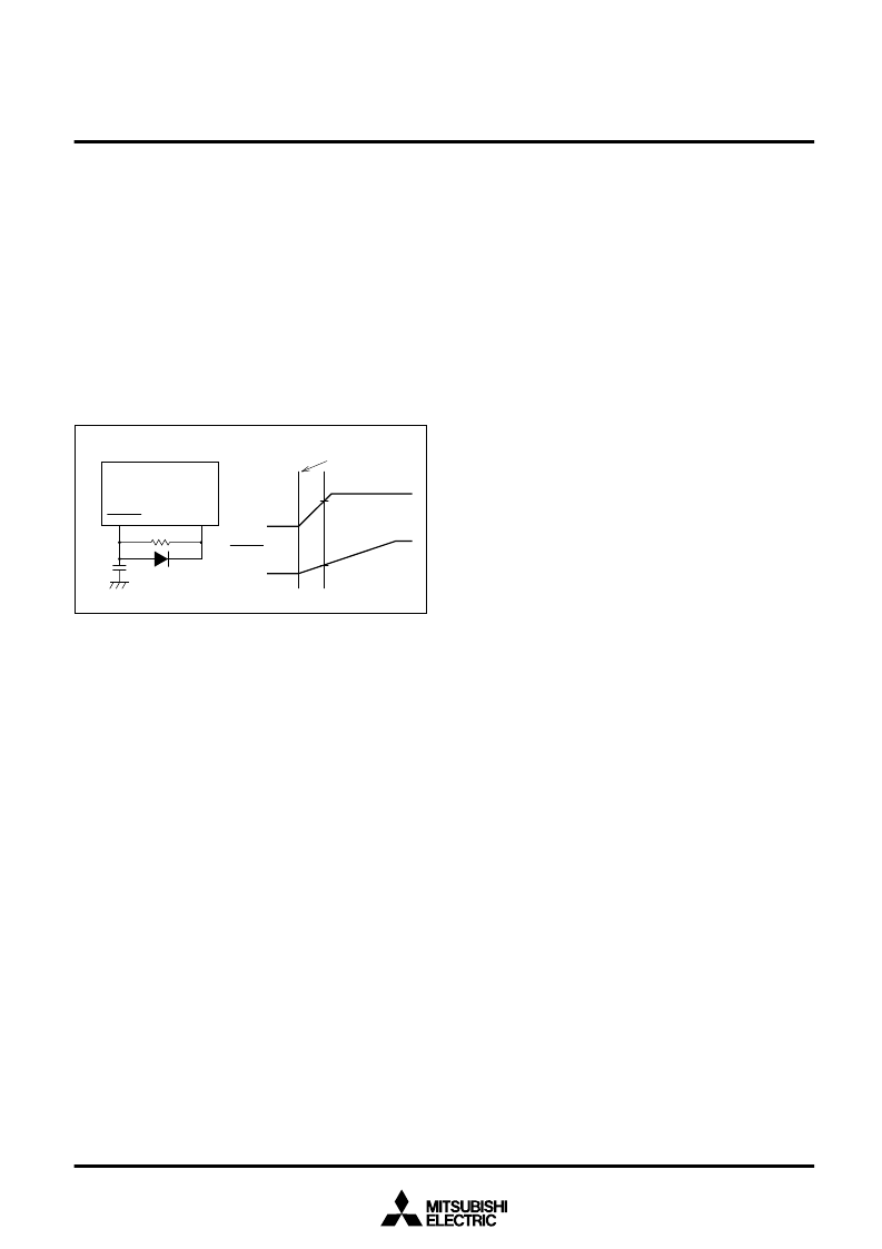
Figure 77 shows an example of a reset circuit. When a stabilized
clock is input from the external to the oscillation circuit, the reset in-
put voltage must be held 0.9V or lower when the supply voltage
reaches 4.5V. When connecting a resonator to the oscillation circuit,
return the reset input voltage from “L” to “H” after the main-clock os-
cillation is fully stabilized
RESET
V
CC
V
CC
RESET
Power on
4.5V
0 V
0 V
0.9V
Fig. 77 Reset circuit example (perform careful evaluation at system
design before using)
INPUT/OUTPUT PINS
Ports P0 to P11 all have the direction register and each bit can be
programmed for input or output. A pin becomes an output pin when
the corresponding bit of direction register is “1”, and an input pin
when it is “0”.
When a pin is programmed for output, the data is written to its port
latch and it is output to the output pin. When a pin is programmed for
output, the contents of the port latch is read instead of the value of
the pin. Accordingly, a previously output value can be read correctly
even when the output “H” voltage is lowered or the output “L” voltage
is raised owing to an external load and others.
A pin programmed as an input pin is floating, and the value input to
the pin can be read. When a pin is programmed as an input pin, the
data is written only in the port latch and the pin remains floating.
Additionally, ports P9
5
, P5
4
to P5
7
include pull-up transistors. The
pull-up function of ports is selected with bits 7 and 6 of the particular
function select register 1. Refer to the section on Interrupts for the
pull-up function.
Figures 78 and 79 show block diagrams of ports P0 to P11 in the
single-chip mode and E output.
Ports P0 to P4, P10 and P11 are also used as pins of address, data
and control signals. Refer to the section on Processor mode for more
details.
相關(guān)PDF資料 |
PDF描述 |
|---|---|
| M37754S4CHP | SINGLE-CHIP 16BIT CMOS MICROCOMPUTER |
| M37754 | SINGLE-CHIP 16BIT CMOS MICROCOMPUTER |
| M37754M8C | Single Chip 16 Bits CMOS Microcomputer(16位單片機(jī)) |
| M37902F8CHP | DIODE SCHOTTKY DUAL COMMON-ANODE 25V 200mW 0.32V-vf 200mA-IFM 1mA-IF 2uA-IR SOT-23 3K/REEL |
| M37902FGCGP | SINGLE-CHIP 16-BIT CMOS MICROCOMPUTER |
相關(guān)代理商/技術(shù)參數(shù) |
參數(shù)描述 |
|---|---|
| M37754S4CHP | 制造商:RENESAS 制造商全稱:Renesas Technology Corp 功能描述:SINGLE-CHIP 16-BIT CMOS MICROCOMPUTER |
| M3775PR-H400CL | 制造商:Bonitron 功能描述:OVERVOLTAGE BRAKING RESISTOR |
| M3775RK-0.75A | 制造商:Bonitron 功能描述:OVERVOLTAGE BRAKING RESISTOR |
| M3775RK-C0.50A | 制造商:Bonitron 功能描述:OVERVOLTAGE BRAKING RESISTOR |
| M3775RK-C0.50B | 制造商:Bonitron 功能描述:OVERVOLTAGE BRAKING RESISTOR |
發(fā)布緊急采購,3分鐘左右您將得到回復(fù)。