- 您現(xiàn)在的位置:買賣IC網(wǎng) > PDF目錄370849 > M37754S4CGP (Mitsubishi Electric Corporation) SINGLE-CHIP 16BIT CMOS MICROCOMPUTER PDF資料下載
參數(shù)資料
| 型號(hào): | M37754S4CGP |
| 廠商: | Mitsubishi Electric Corporation |
| 英文描述: | SINGLE-CHIP 16BIT CMOS MICROCOMPUTER |
| 中文描述: | 單芯片16位微機(jī)的CMOS |
| 文件頁(yè)數(shù): | 38/114頁(yè) |
| 文件大小: | 1116K |
| 代理商: | M37754S4CGP |
第1頁(yè)第2頁(yè)第3頁(yè)第4頁(yè)第5頁(yè)第6頁(yè)第7頁(yè)第8頁(yè)第9頁(yè)第10頁(yè)第11頁(yè)第12頁(yè)第13頁(yè)第14頁(yè)第15頁(yè)第16頁(yè)第17頁(yè)第18頁(yè)第19頁(yè)第20頁(yè)第21頁(yè)第22頁(yè)第23頁(yè)第24頁(yè)第25頁(yè)第26頁(yè)第27頁(yè)第28頁(yè)第29頁(yè)第30頁(yè)第31頁(yè)第32頁(yè)第33頁(yè)第34頁(yè)第35頁(yè)第36頁(yè)第37頁(yè)當(dāng)前第38頁(yè)第39頁(yè)第40頁(yè)第41頁(yè)第42頁(yè)第43頁(yè)第44頁(yè)第45頁(yè)第46頁(yè)第47頁(yè)第48頁(yè)第49頁(yè)第50頁(yè)第51頁(yè)第52頁(yè)第53頁(yè)第54頁(yè)第55頁(yè)第56頁(yè)第57頁(yè)第58頁(yè)第59頁(yè)第60頁(yè)第61頁(yè)第62頁(yè)第63頁(yè)第64頁(yè)第65頁(yè)第66頁(yè)第67頁(yè)第68頁(yè)第69頁(yè)第70頁(yè)第71頁(yè)第72頁(yè)第73頁(yè)第74頁(yè)第75頁(yè)第76頁(yè)第77頁(yè)第78頁(yè)第79頁(yè)第80頁(yè)第81頁(yè)第82頁(yè)第83頁(yè)第84頁(yè)第85頁(yè)第86頁(yè)第87頁(yè)第88頁(yè)第89頁(yè)第90頁(yè)第91頁(yè)第92頁(yè)第93頁(yè)第94頁(yè)第95頁(yè)第96頁(yè)第97頁(yè)第98頁(yè)第99頁(yè)第100頁(yè)第101頁(yè)第102頁(yè)第103頁(yè)第104頁(yè)第105頁(yè)第106頁(yè)第107頁(yè)第108頁(yè)第109頁(yè)第110頁(yè)第111頁(yè)第112頁(yè)第113頁(yè)第114頁(yè)
38
PRELIMINARY
Notice: This is not a final specification.
Some parametric limits are subject to change.
MITSUBISHI MICROCOMPUTERS
M37754M8C-XXXGP, M37754M8C-XXXHP
M37754S4CGP, M37754S4CHP
SINGLE-CHIP 16-BIT CMOS MICROCOMPUTER
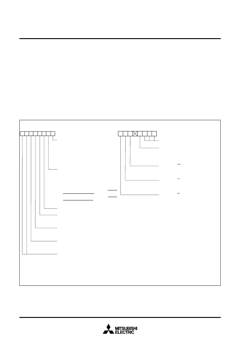
When writing data to the dead-time timer (address 1B
16
), the data is
written to the reload register shared by three dead-time timers.
When the dead-time timers catch the start trigger from the respec-
tive timers, the reload register contents are transferred to its counter
and the dead-time timer decrements with the clock source selected
by bits 6 and 7 of pulse output data register (address 1C
16
). Addition-
ally, this timer can accept another trigger before completion of the
preceding trigger operation. In this case, after transferring the reload
register contents to the dead-time timer at acceptance of the trigger,
the value is decremented.
The dead-time timer operates as a one-shot timer. Accordingly, this
timer starts pulse output when the trigger is caught, and finishes
pulse output and stops operation when its contents become “00
16
”,
and waits next trigger.
Pulse output data register 1 1C
16
V-phase output polarity set buffer
(Three-phase mode 0)
0 : “H” output
1 : “L” output
Interrupt request interval set bit
(Three-phase mode 1)
0 : At every second time
1 : At every fourth time
U-phase output polarity set buffer
(Three-phase mode 0)
0 : “H” output
1 : “L” output
Interrupt validity output select bit
(Three-phase mode 1)
0 : Timer B2 interrupt request generated at each
even-numbered underflow of timer B2.
1 : Timer B2 interrupt request generated at each
odd-numbered underflow of timer B2.
: Not used in three-phase waveform mode
“H” output of W-phase fix buffer
0 : Released from fixed output
1 : “H” output fixed
“H” output of V-phase fix buffer
0 : Released from fixed output
1 : “H” output fixed
“H” output of U-phase fix buffer
0 : Released from fixed output
1 : “H” output fixed
Clock-source-of-dead-time timer select bits
00 : Pf
2
selected
01 : Pf
4
selected
10 : Pf
8
selected
11 : Do not select.
7
6
5
4
3
2
×
1
0
Address
Pulse output data register 0 1D
16
: Not used in three-phase waveform mode
(Valid in three-phase mode 0)
W-phase output polarity set buffer
0 : “H” output
1 : “L” output
“H” output of W-phase fix buffer
0 : Released from fixed output
1 : “H” output fixed
“H” output of V-phase fix buffer
0 : Released from fixed output
1 : “H” output fixed
“H” output of U-phase fix buffer
0 : Released from fixed output
1 : “H” output fixed
7
6
5
4
3
2
×
1
×
0
×
Address
Note :
Only when bit 5 of the particular function select register 1 (in Fig. 15)
is set to “1”, these registers’ contents can be changed from the status
during reset (in Fig.76).
Fig. 44 Bit configuration of pulse output data registers 1 and 0 in three-phase waveform mode
In the three-phase waveform mode, setting bit 7 of the waveform out-
put mode register (address 1A
16
) to “1” makes positive waveforms
(U, V, W phases) and their negative waveforms (U, V, W phases)
output from the respective ports. When that bit is “0”, their ports are
floating. That bit is cleared to “0” by inputting falling edge to the INT
0
pin or reset other than clearing by an instruction..
Additionally, setting bits 5 to 3 of the pulse output data register 1 (ad-
dress 1C
16
) to “1” makes the corresponding positive waveforms
fixed to “H”, and setting bits 7 to 5 of the pulse output data register 0
(address 1D
16
) to “1” makes the corresponding negative waveforms
fixed to “H”.
When selecting the three-phase waveform mode, INT
0
pin become
input-only pin.
相關(guān)PDF資料 |
PDF描述 |
|---|---|
| M37754S4CHP | SINGLE-CHIP 16BIT CMOS MICROCOMPUTER |
| M37754 | SINGLE-CHIP 16BIT CMOS MICROCOMPUTER |
| M37754M8C | Single Chip 16 Bits CMOS Microcomputer(16位單片機(jī)) |
| M37902F8CHP | DIODE SCHOTTKY DUAL COMMON-ANODE 25V 200mW 0.32V-vf 200mA-IFM 1mA-IF 2uA-IR SOT-23 3K/REEL |
| M37902FGCGP | SINGLE-CHIP 16-BIT CMOS MICROCOMPUTER |
相關(guān)代理商/技術(shù)參數(shù) |
參數(shù)描述 |
|---|---|
| M37754S4CHP | 制造商:RENESAS 制造商全稱:Renesas Technology Corp 功能描述:SINGLE-CHIP 16-BIT CMOS MICROCOMPUTER |
| M3775PR-H400CL | 制造商:Bonitron 功能描述:OVERVOLTAGE BRAKING RESISTOR |
| M3775RK-0.75A | 制造商:Bonitron 功能描述:OVERVOLTAGE BRAKING RESISTOR |
| M3775RK-C0.50A | 制造商:Bonitron 功能描述:OVERVOLTAGE BRAKING RESISTOR |
| M3775RK-C0.50B | 制造商:Bonitron 功能描述:OVERVOLTAGE BRAKING RESISTOR |
發(fā)布緊急采購(gòu),3分鐘左右您將得到回復(fù)。