- 您現(xiàn)在的位置:買賣IC網(wǎng) > PDF目錄224000 > HYS64T16000HDL-2.5-A (INFINEON TECHNOLOGIES AG) 16M X 64 DDR DRAM MODULE, 0.4 ns, DMA200 PDF資料下載
參數(shù)資料
| 型號(hào): | HYS64T16000HDL-2.5-A |
| 廠商: | INFINEON TECHNOLOGIES AG |
| 元件分類: | DRAM |
| 英文描述: | 16M X 64 DDR DRAM MODULE, 0.4 ns, DMA200 |
| 封裝: | GREEN, SODIMM-200 |
| 文件頁數(shù): | 21/46頁 |
| 文件大?。?/td> | 833K |
| 代理商: | HYS64T16000HDL-2.5-A |
第1頁第2頁第3頁第4頁第5頁第6頁第7頁第8頁第9頁第10頁第11頁第12頁第13頁第14頁第15頁第16頁第17頁第18頁第19頁第20頁當(dāng)前第21頁第22頁第23頁第24頁第25頁第26頁第27頁第28頁第29頁第30頁第31頁第32頁第33頁第34頁第35頁第36頁第37頁第38頁第39頁第40頁第41頁第42頁第43頁第44頁第45頁第46頁
HYS64T[16/32/64]0xxxHDL–[2.5/3.7/5]–A
Small Outline DDR2 SDRAM Modules
Electrical Characteristics
Data Sheet
25
Rev. 1.1, 2005-06
02182004-HWZ1-64OM
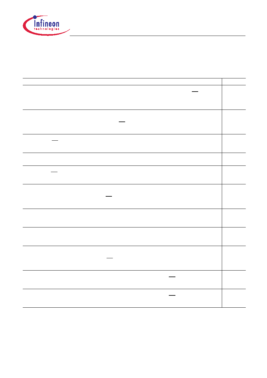
3.4
I
DD Specifications and Conditions
Table 19
I
DD Measurement Conditions
1)2)3)4)5)6)
Parameter
Symbol
Operating Current 0
One bank Active - Precharge;
t
CK = tCK.MIN, tRC = tRC.MIN, tRAS = tRAS.MIN, CKE is HIGH, CS is HIGH
between valid commands. Address and control inputs are SWITCHING, Databus inputs are
SWITCHING.
I
DD0
Operating Current 1
One bank Active - Read - Precharge;
I
OUT = 0 mA, BL = 4, tCK = tCK.MIN, tRC = tRC.MIN, tRAS = tRAS.MIN,
t
RCD = tRCD.MIN, AL = 0, CL = CLMIN; CKE is HIGH, CS is HIGH between valid commands. Address and
control inputs are SWITCHING, Databus inputs are SWITCHING.
I
DD1
Precharge Standby Current
All banks idle; CS is HIGH; CKE is HIGH;
t
CK = tCK.MIN; Other control and address inputs are
SWITCHING, Data bus inputs are SWITCHING.
I
DD2N
Precharge Power-Down Current
Other control and address inputs are STABLE, Data bus inputs are FLOATING.
I
DD2P
Precharge Quiet Standby Current
All banks idle; CS is HIGH; CKE is HIGH;
t
CK = tCK.MIN; Other control and address inputs are STABLE,
Data bus inputs are FLOATING.
I
DD2Q
Active Standby Current
Burst Read: All banks open; Continuous burst reads; BL = 4; AL = 0, CL = CLMIN; tCK = tCK.MIN;
t
RAS = tRAS.MAX, tRP = tRP.MIN; CKE is HIGH, CS is HIGH between valid commands. Address inputs are
SWITCHING; Data Bus inputs are SWITCHING;
I
OUT = 0 mA.
I
DD3N
Active Power-Down Current
All banks open;
t
CK = tCK.MIN, CKE is LOW; Other control and address inputs are STABLE, Data bus
inputs are FLOATING. MRS A12 bit is set to LOW (Fast Power-down Exit);
I
DD3P(0)
Active Power-Down Current
All banks open; tCK = tCK.MIN, CKE is LOW; Other control and address inputs are STABLE, Data bus
inputs are FLOATING. MRS A12 bit is set to HIGH (Slow Power-down Exit);
I
DD3P(1)
Operating Current
urst Write: All banks open; Continuous burst writes; BL = 4; AL = 0, CL = CLMIN; tCK = tCK.MIN;
t
RAS = tRAS.MAX., tRP = tRP.MAX; CKE is HIGH, CS is HIGH between valid commands. Address inputs are
SWITCHING; Data Bus inputs are SWITCHING;
I
DD4W
Burst Refresh Current
t
CK = tCK.MIN., Refresh command every tRFC = tRFC.MIN interval, CKE is HIGH, CS is HIGH between valid
commands, Other control and address inputs are SWITCHING, Data bus inputs are SWITCHING.
I
DD5B
Distributed Refresh Current
t
CK = tCK.MIN., Refresh command every tRFC = tREFI interval, CKE is LOW and CS is HIGH between valid
commands, Other control and address inputs are SWITCHING, Data bus inputs are SWITCHING.
I
DD5D
相關(guān)PDF資料 |
PDF描述 |
|---|---|
| HYS72D64020GR-7-X | 64M X 72 DDR DRAM MODULE, 0.75 ns, DMA184 |
| HYS72D64020GR-7.5-X | 64M X 72 DDR DRAM MODULE, 0.75 ns, DMA184 |
| HYS72T128000EU-2.5-C2 | 128M X 72 DDR DRAM MODULE, 0.4 ns, DMA240 |
| HYS72T64000EP-3.7-B2 | 64M X 72 DDR DRAM MODULE, DMA240 |
| HZ20-1 | 19.25 V, 0.5 W, SILICON, UNIDIRECTIONAL VOLTAGE REGULATOR DIODE, DO-35 |
相關(guān)代理商/技術(shù)參數(shù) |
參數(shù)描述 |
|---|---|
| HYS64T16000HU | 制造商:QIMONDA 制造商全稱:QIMONDA 功能描述:240-Pin Unbuffered DDR2 SDRAM Modules |
| HYS64T16000HU-3.7-A | 制造商:QIMONDA 制造商全稱:QIMONDA 功能描述:240-Pin Unbuffered DDR2 SDRAM Modules |
| HYS64T16000HU-5-A | 制造商:QIMONDA 制造商全稱:QIMONDA 功能描述:240-Pin Unbuffered DDR2 SDRAM Modules |
| HYS64T256020EDL | 制造商:QIMONDA 制造商全稱:QIMONDA 功能描述:200-Pin SO-DIMM DDR2 SDRAM Modules |
| HYS64T256020EDL-2.5-C | 制造商:QIMONDA 制造商全稱:QIMONDA 功能描述:200-Pin SO-DIMM DDR2 SDRAM Modules |
發(fā)布緊急采購,3分鐘左右您將得到回復(fù)。