- 您現(xiàn)在的位置:買賣IC網 > PDF目錄375249 > AD9852ASQ (ANALOG DEVICES INC) CMOS 300 MHz Complete-DDS PDF資料下載
參數(shù)資料
| 型號: | AD9852ASQ |
| 廠商: | ANALOG DEVICES INC |
| 元件分類: | XO, clock |
| 英文描述: | CMOS 300 MHz Complete-DDS |
| 中文描述: | PLL FREQUENCY SYNTHESIZER, 30 MHz, PQFP80 |
| 封裝: | MS-026-BEC, LQFP-80 |
| 文件頁數(shù): | 28/42頁 |
| 文件大?。?/td> | 424K |
| 代理商: | AD9852ASQ |
第1頁第2頁第3頁第4頁第5頁第6頁第7頁第8頁第9頁第10頁第11頁第12頁第13頁第14頁第15頁第16頁第17頁第18頁第19頁第20頁第21頁第22頁第23頁第24頁第25頁第26頁第27頁當前第28頁第29頁第30頁第31頁第32頁第33頁第34頁第35頁第36頁第37頁第38頁第39頁第40頁第41頁第42頁
AD9852
–28–
REV. 0
Instruction Byte
The instruction byte contains the following information.
Table VIII. Instruction Byte Information
MSB
D6
D5
D4
D3
D2
D1
LSB
R/
W
X
X
X
A3
A2
A1
A0
R/
W
—Bit 7 of the instruction byte determines whether a read or
write data transfer will occur after the instruction byte write. Logic
high indicates read operation. Logic zero indicates a write operation.
Bits 6, 5, and 4 of the instruction byte are don’t care.
A3, A2, A1, A0—Bits 3, 2, 1, 0 of the instruction byte determine
which register is accessed during the data transfer portion of the
communications cycle. See Table VIII for register address details.
SERIAL INTERFACE PORT PIN DESCRIPTION
SCLK
Serial Clock (Pin 21). The serial clock pin is used to synchronize
data to and from the AD9852 and to run the internal state
machines. SCLK maximum frequency is 10 MHz.
CS
Chip Select (Pin 22). Active low input that allows more than
one device on the same serial communications lines. The SDO
and SDIO pins will go to a high impedance state when this
input is high. If driven high during any communications cycle,
that cycle is suspended until
CS
is reactivated low. Chip Select
can be tied low in systems that maintain control of SCLK.
SDIO
Serial Data I/O (Pin 19). Data is always written into the AD9852
on this pin. However, this pin can be used as a bidirectional
data line. The configuration of this pin is controlled by Bit 0 of
register address 20h. The default is logic zero, which configures
the SDIO pin as bidirectional.
SDO
Serial Data Out (Pin 18). Data is read from this pin for proto-
cols that use separate lines for transmitting and receiving data.
In the case where the AD9852 operates in a single bidirectional
I/O mode, this pin does not output data and is set to a high
impedance state.
IO RESET
Synchronize I/O Port (Pin 17). Synchronizes the I/O port state
machines without affecting the addressable registers contents.
An active high input on IO RESET pin causes the current commu-
nication cycle to terminate. After IO RESET returns low (Logic
0) another communication cycle may begin, starting with the
instruction byte write.
NOTES ON SERIAL PORT OPERATION
The AD9852 serial port configuration bits reside in Bits 1 and 0
of register address 20h. It is important to note that the con-
figuration changes
immediately
upon a valid I/O update. For
multibyte transfers, writing this register may occur during the
middle of a communication cycle. Care must be taken to com-
pensate for this new configuration for the remainder of the
current communication cycle.
The system must maintain synchronization with the AD9852 or
the internal control logic will not be able to recognize further
instructions. For example, if the system sends the instruction to
write a 2-byte register, then pulses the SCLK pin for a 3-byte
register (24 additional SCLK rising edges), communication
synchronization is lost. In this case, the first 16 SCLK rising edges
after the instruction cycle will properly write the first two data
bytes into the AD9852, but the next eight rising SCLK edges
are interpreted as the next instruction byte, NOT the final byte
of the previous communication cycle.
In the case where synchronization is lost between the system and
the AD9852, the IO RESET pin provides a means to reestablish
synchronization without reinitializing the entire chip. Asserting
the IO RESET pin (active high) resets the AD9852 serial port state
machine, terminating the current IO operation and putting the
device into a state in which the next eight SCLK rising edges
are understood to be an instruction byte. The SYNC IO pin
must be deasserted (low) before the next instruction byte write can
begin. Any information that had been written to the AD9852
registers during a valid communication cycle prior to loss of
synchronization will remain intact.
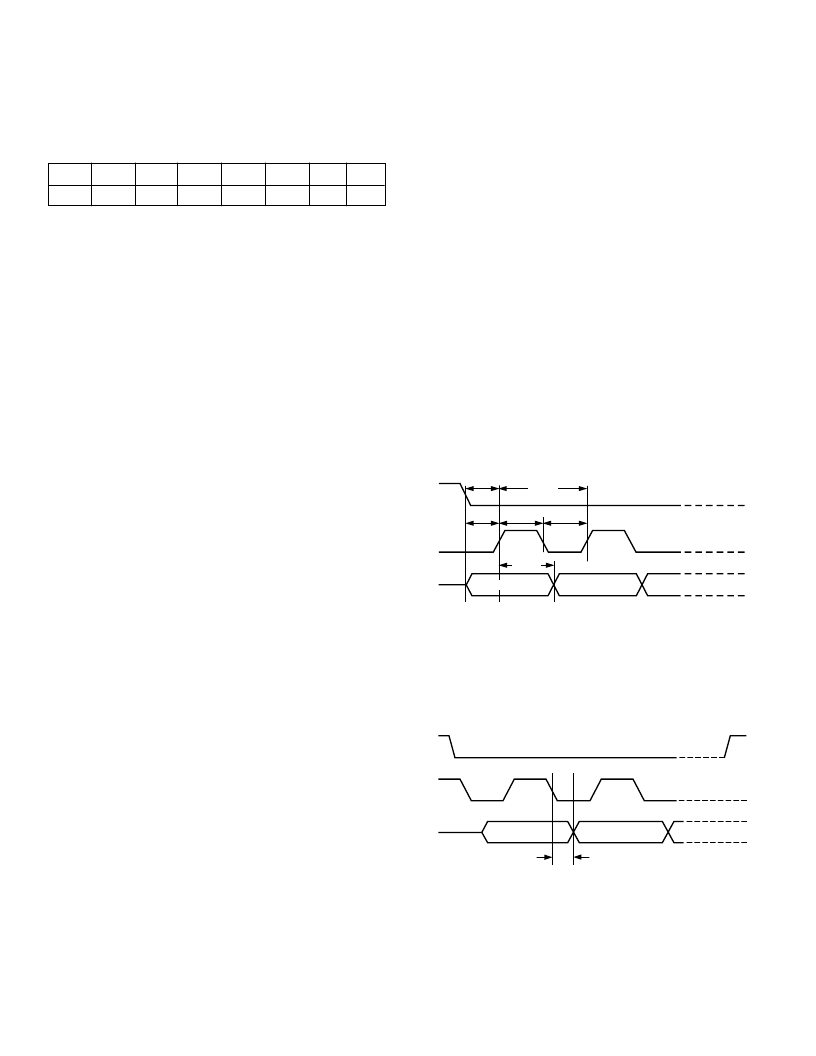
CS
SCLK
SDIO
t
PRE
t
DSU
t
SCLKPWH
t
SCLKPWL
t
SCLK
t
DHLD
2ND BIT
1ST BIT
SYMBOL
T
PRE
T
SCLK
T
DSU
T
SCLKPWH
T
SCLKPWL
T
DHLD
MIN
30ns
100ns
30ns
40ns
40ns
0ns
DEFINITION
CS
SETUP TIME
PERIOD OF SERIAL DATA CLOCK
SERIAL DATA SETUP TIME
SERIAL DATA CLOCK PULSEWIDTH HIGH
SERIAL DATA CLOCK PULSEWIDTH LOW
SERIAL DATA HOLD TIME
Figure 53. Timing Diagram for Data Write to AD9852
t
DV
1ST BIT
2ND BIT
SDIO
SDO
SCLK
CS
SYMBOL
T
DV
MAX
30ns
DEFINITION
DATA VALID TIME
Figure 54. Timing Diagram for Read from AD9852
相關PDF資料 |
PDF描述 |
|---|---|
| AD9852AST | CMOS 300 MHz Complete-DDS |
| AD9853-45PCB | Programmable Digital OPSK/16-QAM Modulator |
| AD9853-65PCB | Programmable Digital OPSK/16-QAM Modulator |
| AD9853AS | Programmable Digital OPSK/16-QAM Modulator |
| AD9854ASQ | CMOS 300 MHz Quadrature Complete-DDS |
相關代理商/技術參數(shù) |
參數(shù)描述 |
|---|---|
| AD9852ASQZ | 制造商:Analog Devices 功能描述:Direct Digital Synthesizer 300MHz 2-DAC 12-Bit Parallel/Serial 80-Pin LQFP |
| AD9852AST | 制造商:Analog Devices 功能描述:Direct Digital Synthesizer 300MHz 2-DAC 12-Bit Parallel/Serial 80-Pin LQFP Tray 制造商:Rochester Electronics LLC 功能描述:200 MHZ C-DDS SYNTHESIZER - Bulk 制造商:Analog Devices 功能描述:IC DDS SYNTHESIZER |
| AD9852ASTZ | 功能描述:IC DDS SYNTHESIZER CMOS 80-LQFP RoHS:是 類別:集成電路 (IC) >> 接口 - 直接數(shù)字合成 (DDS) 系列:- 產品變化通告:Product Discontinuance 27/Oct/2011 標準包裝:2,500 系列:- 分辨率(位):10 b 主 fclk:25MHz 調節(jié)字寬(位):32 b 電源電壓:2.97 V ~ 5.5 V 工作溫度:-40°C ~ 85°C 安裝類型:表面貼裝 封裝/外殼:16-TSSOP(0.173",4.40mm 寬) 供應商設備封裝:16-TSSOP 包裝:帶卷 (TR) |
| AD9852ASTZ | 制造商:Analog Devices 功能描述:IC DDS 100MHZ LQFP-80 |
| AD9852ASTZ1 | 制造商:AD 制造商全稱:Analog Devices 功能描述:CMOS 300 MSPS Complete DDS |
發(fā)布緊急采購,3分鐘左右您將得到回復。