- 您現在的位置:買賣IC網 > PDF目錄375249 > AD9852ASQ (ANALOG DEVICES INC) CMOS 300 MHz Complete-DDS PDF資料下載
參數資料
| 型號: | AD9852ASQ |
| 廠商: | ANALOG DEVICES INC |
| 元件分類: | XO, clock |
| 英文描述: | CMOS 300 MHz Complete-DDS |
| 中文描述: | PLL FREQUENCY SYNTHESIZER, 30 MHz, PQFP80 |
| 封裝: | MS-026-BEC, LQFP-80 |
| 文件頁數: | 23/42頁 |
| 文件大?。?/td> | 424K |
| 代理商: | AD9852ASQ |
第1頁第2頁第3頁第4頁第5頁第6頁第7頁第8頁第9頁第10頁第11頁第12頁第13頁第14頁第15頁第16頁第17頁第18頁第19頁第20頁第21頁第22頁當前第23頁第24頁第25頁第26頁第27頁第28頁第29頁第30頁第31頁第32頁第33頁第34頁第35頁第36頁第37頁第38頁第39頁第40頁第41頁第42頁
AD9852
–23–
REV. 0
4. Continue chirp by reversing direction and returning to the
previous, or another, destination frequency in a linear or user-
directed manner. If this involves going down in frequency, a
negative 48-bit Delta Frequency Word (the MSB is set to “1”)
must be loaded into registers 10–15 hex. Any decreasing fre-
quency step of the Delta Frequency Word requires the MSB to
be set to logic high.
5. Continue chirp by immediately returning to the F1 beginning
frequency in a sawtooth fashion and repeat the previous chirp
process again. This is where CLR ACC1 control bit is used.
An automatic, repeating chirp can be setup using the 32-bit
Update Clock to issue CLR ACC1 commands at precise time
intervals. Adjusting the timing intervals or changing the Delta
Frequency Word will change the chirp range. It is incumbent
upon the user to balance the chirp duration and frequency
resolution to achieve the proper frequency range.
BPSK (Mode 100)
Binary, biphase, or bipolar phase shift keying is a means to rapidly
select between two preprogramming 14-bit output phase offsets
that will identically affect both the I and Q outputs of the AD9852.
The logic-state of Pin 29, BPSK pin, controls the selection of
Phase Adjust register number 1 or 2. When low, Pin 29 selects
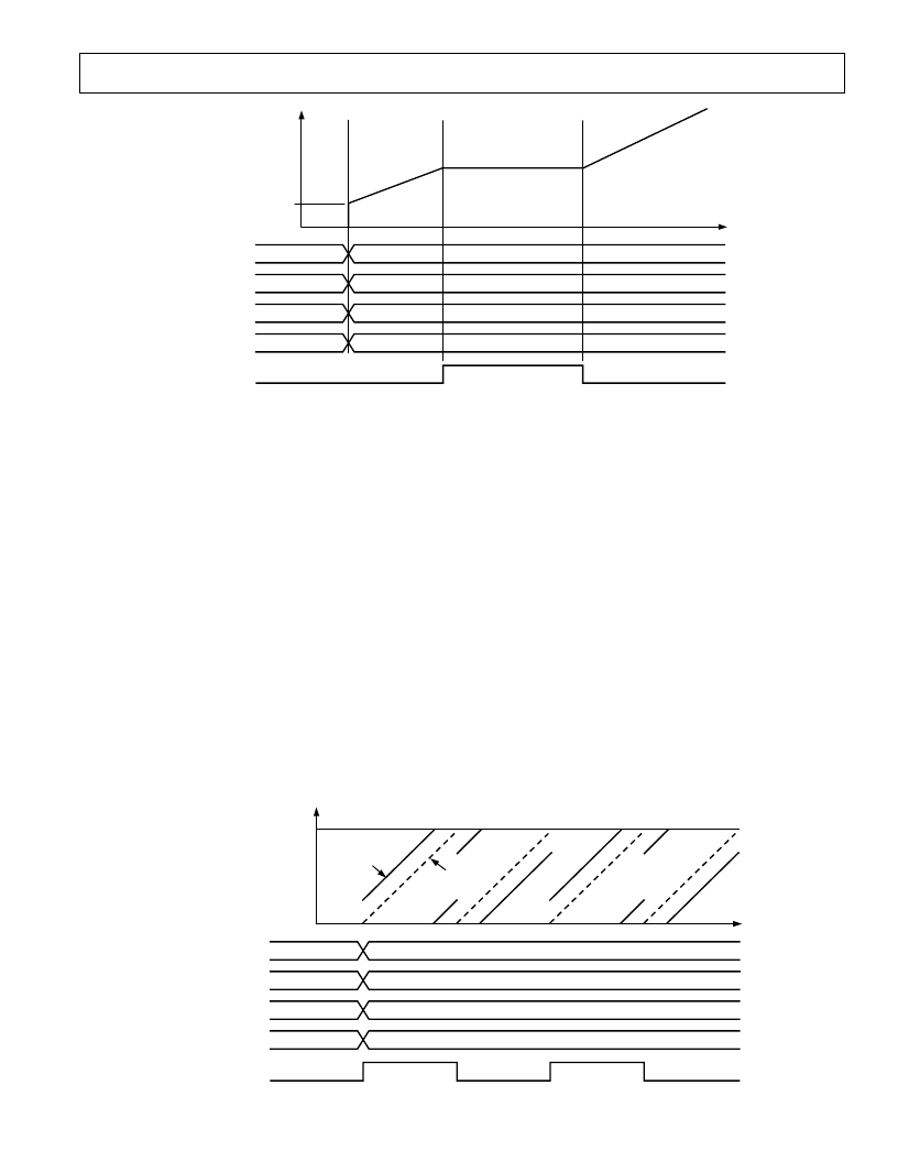
HOLD
F1
0
F
MODE
TW1
DFW
000 (DEFAULT)
0
RAMP RATE
011 (CHIRP)
F1
DELTA FREQUENCY WORD
RAMP RATE
Figure 47. Illustration of HOLD Function
Phase Adjust register 1; when high, Phase Adjust register 2 is
selected. Figure 48 illustrates phase changes made to four cycles
of an output carrier.
Basic BPSK programming steps:
1. Program a carrier frequency into Frequency Tuning Word 1.
2. Program appropriate 14-bit phase words in Phase Adjust
registers 1 and 2.
3. Attach BPSK data source to Pin 29.
4. Activate I/O Update pulse when ready.
If phase shift keying is not the objective, but rather a broader
range of phase offsets is needed, the user should select the Single-
Tone mode and program Phase Adjust register 1 using the serial or
high-speed parallel programming bus.
I/O Port Buffers
—100 MHz, 8-bit parallel or 10 MHz serial
loading, SPI-compatible. The programming mode is selected
externally via the serial/parallel (S/P Select) pin. I/O Buffers can
be written to, or read from, according to the signals supplied to
the Read (RDB) and Write pins (WRB) and the 6-bit address
(A0–A5) in the parallel mode or to CSB, SCLK and SDIO pins
in the Serial mode.
BPSK DATA
360
0
P
MODE
FTW1
PHASE ADJUST 1
000 (DEFAULT)
0
PHASE ADJUST 2
100 (BPSK)
F1
270 DEGREES
90 DEGREES
PHASE AFTER
ONSET
PHASE BEFORE
ONSET
Figure 48. BPSK Mode
相關PDF資料 |
PDF描述 |
|---|---|
| AD9852AST | CMOS 300 MHz Complete-DDS |
| AD9853-45PCB | Programmable Digital OPSK/16-QAM Modulator |
| AD9853-65PCB | Programmable Digital OPSK/16-QAM Modulator |
| AD9853AS | Programmable Digital OPSK/16-QAM Modulator |
| AD9854ASQ | CMOS 300 MHz Quadrature Complete-DDS |
相關代理商/技術參數 |
參數描述 |
|---|---|
| AD9852ASQZ | 制造商:Analog Devices 功能描述:Direct Digital Synthesizer 300MHz 2-DAC 12-Bit Parallel/Serial 80-Pin LQFP |
| AD9852AST | 制造商:Analog Devices 功能描述:Direct Digital Synthesizer 300MHz 2-DAC 12-Bit Parallel/Serial 80-Pin LQFP Tray 制造商:Rochester Electronics LLC 功能描述:200 MHZ C-DDS SYNTHESIZER - Bulk 制造商:Analog Devices 功能描述:IC DDS SYNTHESIZER |
| AD9852ASTZ | 功能描述:IC DDS SYNTHESIZER CMOS 80-LQFP RoHS:是 類別:集成電路 (IC) >> 接口 - 直接數字合成 (DDS) 系列:- 產品變化通告:Product Discontinuance 27/Oct/2011 標準包裝:2,500 系列:- 分辨率(位):10 b 主 fclk:25MHz 調節(jié)字寬(位):32 b 電源電壓:2.97 V ~ 5.5 V 工作溫度:-40°C ~ 85°C 安裝類型:表面貼裝 封裝/外殼:16-TSSOP(0.173",4.40mm 寬) 供應商設備封裝:16-TSSOP 包裝:帶卷 (TR) |
| AD9852ASTZ | 制造商:Analog Devices 功能描述:IC DDS 100MHZ LQFP-80 |
| AD9852ASTZ1 | 制造商:AD 制造商全稱:Analog Devices 功能描述:CMOS 300 MSPS Complete DDS |
發(fā)布緊急采購,3分鐘左右您將得到回復。