- 您現(xiàn)在的位置:買(mǎi)賣(mài)IC網(wǎng) > PDF目錄360656 > 9S12KT256DGV1 MC9S12KT256 Device User Guide PDF資料下載
參數(shù)資料
| 型號(hào): | 9S12KT256DGV1 |
| 英文描述: | MC9S12KT256 Device User Guide |
| 中文描述: | MC9S12KT256設(shè)備用戶(hù)指南 |
| 文件頁(yè)數(shù): | 62/126頁(yè) |
| 文件大小: | 7307K |
| 代理商: | 9S12KT256DGV1 |
第1頁(yè)第2頁(yè)第3頁(yè)第4頁(yè)第5頁(yè)第6頁(yè)第7頁(yè)第8頁(yè)第9頁(yè)第10頁(yè)第11頁(yè)第12頁(yè)第13頁(yè)第14頁(yè)第15頁(yè)第16頁(yè)第17頁(yè)第18頁(yè)第19頁(yè)第20頁(yè)第21頁(yè)第22頁(yè)第23頁(yè)第24頁(yè)第25頁(yè)第26頁(yè)第27頁(yè)第28頁(yè)第29頁(yè)第30頁(yè)第31頁(yè)第32頁(yè)第33頁(yè)第34頁(yè)第35頁(yè)第36頁(yè)第37頁(yè)第38頁(yè)第39頁(yè)第40頁(yè)第41頁(yè)第42頁(yè)第43頁(yè)第44頁(yè)第45頁(yè)第46頁(yè)第47頁(yè)第48頁(yè)第49頁(yè)第50頁(yè)第51頁(yè)第52頁(yè)第53頁(yè)第54頁(yè)第55頁(yè)第56頁(yè)第57頁(yè)第58頁(yè)第59頁(yè)第60頁(yè)第61頁(yè)當(dāng)前第62頁(yè)第63頁(yè)第64頁(yè)第65頁(yè)第66頁(yè)第67頁(yè)第68頁(yè)第69頁(yè)第70頁(yè)第71頁(yè)第72頁(yè)第73頁(yè)第74頁(yè)第75頁(yè)第76頁(yè)第77頁(yè)第78頁(yè)第79頁(yè)第80頁(yè)第81頁(yè)第82頁(yè)第83頁(yè)第84頁(yè)第85頁(yè)第86頁(yè)第87頁(yè)第88頁(yè)第89頁(yè)第90頁(yè)第91頁(yè)第92頁(yè)第93頁(yè)第94頁(yè)第95頁(yè)第96頁(yè)第97頁(yè)第98頁(yè)第99頁(yè)第100頁(yè)第101頁(yè)第102頁(yè)第103頁(yè)第104頁(yè)第105頁(yè)第106頁(yè)第107頁(yè)第108頁(yè)第109頁(yè)第110頁(yè)第111頁(yè)第112頁(yè)第113頁(yè)第114頁(yè)第115頁(yè)第116頁(yè)第117頁(yè)第118頁(yè)第119頁(yè)第120頁(yè)第121頁(yè)第122頁(yè)第123頁(yè)第124頁(yè)第125頁(yè)第126頁(yè)
Device User Guide — 9S12KT256DGV1/D V01.09
62
Freescale Semiconductor
2.3.10 PB[7:0] / ADDR[7:0] / DATA[7:0] — Port B I/O Pins
PB7-PB0 are general purpose input or output pins. In MCU expanded modes of operation, these pins are
used for the multiplexed external address and data bus.
2.3.11 PE7 / NOACC / XCLKS — Port E I/O Pin 7
PE7 is a general purpose input or output pin. During MCU expanded modes of operation, the NOACC
signal, when enabled, is used to indicate that the current bus cycle is an unused or “free” cycle. This signal
will assert when the CPU is not using the bus.
The XCLKS is an input signal which controls whether a crystal in combination with the internal Loop
Controlled Pierce (low power) oscillator is used or whether Full Swing Pierce oscillator/external clock
circuitry is used. The state of this pin is latched at the rising edge of RESET. If the input is a logic low the
EXTAL pin is configured for an external clock drive or Full Swing Pierce Oscillator. If input is a logic
high a Loop Controlled Pierce oscillator circuit is configured on EXTAL and XTAL. Since this pin is an
input with a pull-up device during reset, if the pin is left floating, the default configuration is a Loop
Controlled Pierce oscillator circuit on EXTAL and XTAL.
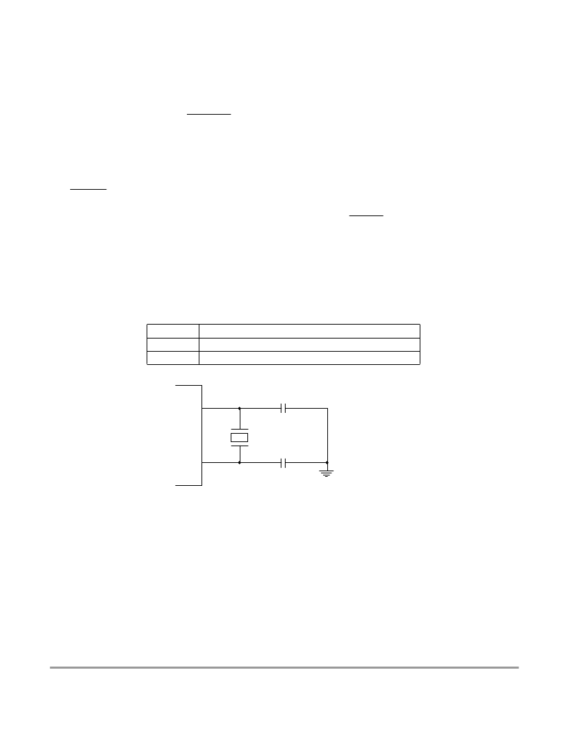
Figure 2-5 Loop Controlled Pierce Oscillator Connections (PE7=1)
Table 2-3 Clock selection based on PE7 during reset
PE7
1
0
Description
Loop Controlled Pierce Oscillator selected
Full Swing Pierce Oscillator or external clock selected
MCU
EXTAL
XTAL
VSSPLL
Crystal or
ceramic resonator
C
8
C
7
相關(guān)PDF資料 |
PDF描述 |
|---|---|
| 9S12T64AF16V1 | 9S12T64 Device Guide |
| 9S12XDP512DGV1 | Device User Guide for Mask Set 0L40V ( First Silicon) |
| 9S12XDP512DGV2 | Device User Guide for Mask Set L15Y - (Second Silicon - Enhanced Feature Set) |
| 9V3 | ELEMENT 10 MICRON E MEDIA |
| 6RS15 | Power-Supply Monitor with Reset |
相關(guān)代理商/技術(shù)參數(shù) |
參數(shù)描述 |
|---|---|
| 9S-12MEFA16-IND | 制造商:Hong Kong Crystal 功能描述:HC49USCRYSTALS METAL CAN |
| 9S12T64AF16V1 | 制造商:未知廠家 制造商全稱(chēng):未知廠家 功能描述:9S12T64 Device Guide |
| 9S12XDP512DGV1 | 制造商:未知廠家 制造商全稱(chēng):未知廠家 功能描述:Device User Guide for Mask Set 0L40V ( First Silicon) |
| 9S12XDP512DGV2 | 制造商:未知廠家 制造商全稱(chēng):未知廠家 功能描述:Device User Guide for Mask Set L15Y - (Second Silicon - Enhanced Feature Set) |
| 9S-14.7456MEFA20-IND | 制造商:Hong Kong Crystal 功能描述:14.7456M,CRYSTAL 制造商:Hong Kong Crystal 功能描述:HC49US CRYSTALS METAL CAN 制造商:Hong Kong Crystal 功能描述:HC49USCRYSTALS METAL CAN |
發(fā)布緊急采購(gòu),3分鐘左右您將得到回復(fù)。