- 您現(xiàn)在的位置:買賣IC網(wǎng) > PDF目錄231493 > W9425G6EH-5I (WINBOND ELECTRONICS CORP) 16M X 16 DDR DRAM, 0.7 ns, PDSO66 PDF資料下載
參數(shù)資料
| 型號: | W9425G6EH-5I |
| 廠商: | WINBOND ELECTRONICS CORP |
| 元件分類: | DRAM |
| 英文描述: | 16M X 16 DDR DRAM, 0.7 ns, PDSO66 |
| 封裝: | 0.400 INCH, ROHS COMPLIANT, TSOP2-66 |
| 文件頁數(shù): | 52/54頁 |
| 文件大?。?/td> | 0K |
| 代理商: | W9425G6EH-5I |
第1頁第2頁第3頁第4頁第5頁第6頁第7頁第8頁第9頁第10頁第11頁第12頁第13頁第14頁第15頁第16頁第17頁第18頁第19頁第20頁第21頁第22頁第23頁第24頁第25頁第26頁第27頁第28頁第29頁第30頁第31頁第32頁第33頁第34頁第35頁第36頁第37頁第38頁第39頁第40頁第41頁第42頁第43頁第44頁第45頁第46頁第47頁第48頁第49頁第50頁第51頁當(dāng)前第52頁第53頁第54頁
W9425G6EH
Publication Release Date:Dec. 03, 2008
- 7 -
Revision A08
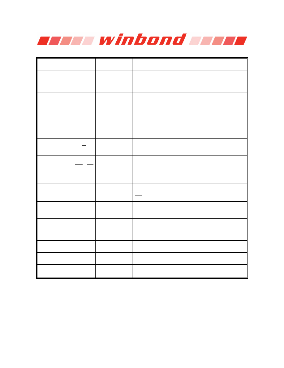
5. PIN DESCRIPTION
PIN NUMBER
PIN
NAME
FUNCTION
DESCRIPTION
28
32,
35
42
A0
A12
Address
Multiplexed pins for row and column address.
Row address: A0
A12.
Column address: A0
A8. (A10 is used for Auto-precharge)
26, 27
BA0, BA1
Bank Select
Select bank to activate during row address latch time, or
bank to read/write during column address latch time.
2, 4, 5, 7, 8, 10,
11, 13, 54, 56, 57,
59, 60, 62, 63, 65
DQ0
DQ15
Data Input/ Output
The DQ0 – DQ15 input and output data are synchronized
with both edges of DQS.
16,51
LDQS,
UDQS
Data Strobe
DQS is Bi-directional signal. DQS is input signal during write
operation and output signal during read operation. It is Edge-
aligned with read data, Center-aligned with write data.
24
CS
Chip Select
Disable or enable the command decoder. When command
decoder is disabled, new command is ignored and previous
operation continues.
23, 22, 21
RAS ,
CAS
, WE
Command Inputs Command inputs (along with CS ) define the command
being entered.
20, 47
LDM, UDM
Write Mask
When DM is asserted “high” in burst write, the input data is
masked. DM is synchronized with both edges of DQS.
45, 46
CLK,
CLK
Differential Clock
Inputs
All address and control input signals are sampled on the
crossing of the positive edge of CLK and negative edge of
CLK
.
44
CKE
Clock Enable
CKE controls the clock activation and deactivation. When
CKE is low, Power Down mode, Suspend mode, or Self
Refresh mode is entered.
49
VREF
Reference Voltage VREF is reference voltage for inputs.
1, 18, 33
VDD
Power (+2.5V)
Power for logic circuit inside DDR SDRAM.
34, 48, 66
VSS
Ground
Ground for logic circuit inside DDR SDRAM.
3, 9, 15, 55, 61
VDDQ
Power (+2.5V) for
I/O Buffer
Separated power from VDD, used for output buffer, to
improve noise.
6, 12, 52, 58, 64
VSSQ
Ground for I/O
Buffer
Separated ground from VSS, used for output buffer, to
improve noise.
14, 17, 19, 25,
43, 50, 53
NC
No Connection
No connection
(NC pin should be connected to GND or
floating)
相關(guān)PDF資料 |
PDF描述 |
|---|---|
| W7NCF02GH11IS8EG | 128M X 16 FLASH 3.3V PROM CARD, 150 ns, UUC |
| WS512K32-55G2UMA | 512K X 32 MULTI DEVICE SRAM MODULE, 55 ns, CQFP68 |
| WS512K32-45G2UM | 512K X 32 MULTI DEVICE SRAM MODULE, 45 ns, CQFP68 |
| WS512K32L-45G4TM | 512K X 32 MULTI DEVICE SRAM MODULE, 45 ns, CQFP68 |
| WS512K32N-35G4TCA | 512K X 32 MULTI DEVICE SRAM MODULE, 35 ns, CQFP68 |
相關(guān)代理商/技術(shù)參數(shù) |
參數(shù)描述 |
|---|---|
| W9425G6JB-5 | 制造商:Winbond Electronics Corp 功能描述:DRAM Chip DDR SDRAM 256M-Bit 16Mx16 2.5V 60-Pin TFBGA 制造商:Winbond Electronics 功能描述:IC MEMORY 制造商:Winbond Electronics Corp 功能描述:IC MEMORY 制造商:Winbond 功能描述:16MX16,256Mb DDRI DRAM ,200MHZ, BGA |
| W9425G6JB-5 TR | 制造商:Winbond Electronics Corp 功能描述:256M DDR SDRAM X16, 200MHZ |
| W9425G6JB-5I | 制造商:Winbond Electronics Corp 功能描述:DRAM Chip DDR SDRAM 256M-Bit 16Mx16 2.5V 制造商:Winbond Electronics 功能描述:IC MEMORY 制造商:Winbond Electronics Corp 功能描述:IC MEMORY |
| W9425G6JB-5I TR | 制造商:Winbond Electronics Corp 功能描述:256M DDR SDRAM X16, 200MHZ, IN |
| W9425G6JH | 制造商:WINBOND 制造商全稱:Winbond 功能描述:4 M × 4 BANKS × 16 BITS DDR SDRAM |
發(fā)布緊急采購,3分鐘左右您將得到回復(fù)。