- 您現(xiàn)在的位置:買(mǎi)賣(mài)IC網(wǎng) > PDF目錄383982 > UPD703201 (NEC Corp.) 32-BIT SINGLE-CHIP MICROCONTROLLERS PDF資料下載
參數(shù)資料
| 型號(hào): | UPD703201 |
| 廠(chǎng)商: | NEC Corp. |
| 英文描述: | 32-BIT SINGLE-CHIP MICROCONTROLLERS |
| 中文描述: | 32位單晶片微控制器 |
| 文件頁(yè)數(shù): | 62/98頁(yè) |
| 文件大?。?/td> | 797K |
| 代理商: | UPD703201 |
第1頁(yè)第2頁(yè)第3頁(yè)第4頁(yè)第5頁(yè)第6頁(yè)第7頁(yè)第8頁(yè)第9頁(yè)第10頁(yè)第11頁(yè)第12頁(yè)第13頁(yè)第14頁(yè)第15頁(yè)第16頁(yè)第17頁(yè)第18頁(yè)第19頁(yè)第20頁(yè)第21頁(yè)第22頁(yè)第23頁(yè)第24頁(yè)第25頁(yè)第26頁(yè)第27頁(yè)第28頁(yè)第29頁(yè)第30頁(yè)第31頁(yè)第32頁(yè)第33頁(yè)第34頁(yè)第35頁(yè)第36頁(yè)第37頁(yè)第38頁(yè)第39頁(yè)第40頁(yè)第41頁(yè)第42頁(yè)第43頁(yè)第44頁(yè)第45頁(yè)第46頁(yè)第47頁(yè)第48頁(yè)第49頁(yè)第50頁(yè)第51頁(yè)第52頁(yè)第53頁(yè)第54頁(yè)第55頁(yè)第56頁(yè)第57頁(yè)第58頁(yè)第59頁(yè)第60頁(yè)第61頁(yè)當(dāng)前第62頁(yè)第63頁(yè)第64頁(yè)第65頁(yè)第66頁(yè)第67頁(yè)第68頁(yè)第69頁(yè)第70頁(yè)第71頁(yè)第72頁(yè)第73頁(yè)第74頁(yè)第75頁(yè)第76頁(yè)第77頁(yè)第78頁(yè)第79頁(yè)第80頁(yè)第81頁(yè)第82頁(yè)第83頁(yè)第84頁(yè)第85頁(yè)第86頁(yè)第87頁(yè)第88頁(yè)第89頁(yè)第90頁(yè)第91頁(yè)第92頁(yè)第93頁(yè)第94頁(yè)第95頁(yè)第96頁(yè)第97頁(yè)第98頁(yè)
Preliminary Product Information U15436EJ1V0PM
62
μ
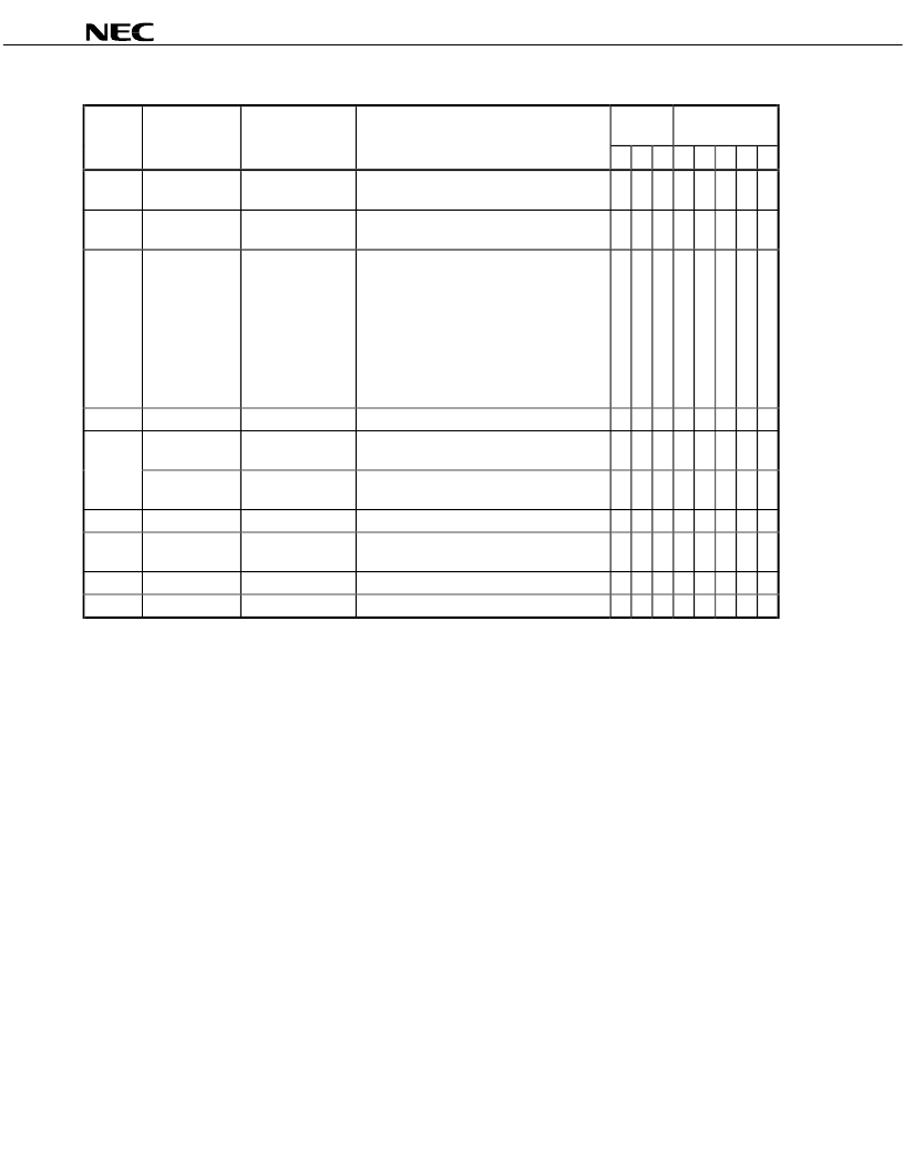
PD703201, 703201Y, 703204, 703204Y, 70F3201, 70F3201Y, 70F3204, 70F3204Y
(6/6)
Execution
Clock
Flags
Mnemonic
Operand
Opcode
Operation
i
r
l
CY OV
S
Z SAT
SXB
reg1
00000000101RRRRR
GR[reg1]
←
sign-extend
(GR[reg1] (7 : 0))
1
1
1
SXH
reg1
00000000111RRRRR
GR[reg1]
←
sign-extend
(GR[reg1] (15 : 0))
1
1
1
TRAP
vector
00000 1111 11iiiii
0000000100000000
EIPC
←
PC+4
(Restored PC)
←
PSW
EIPSW
ECR.EICC
←
Interrupt Code
PSW.EP
←
1
PSW.ID
←
1
PC
←
00000040H
(when vector is 00H to
0FH)
00000050H
(when vector is 10H to
1FH)
3
3
3
TST
reg1,reg2
rrrrr001011RRRRR
result
←
GR[reg2] AND GR[reg1]
1
1
1
0
×
×
bit#3,disp16[reg1]
11bbb111110RRRRR
dddddddddddddddd
adr
←
GR[reg1]+sign-extend(disp16)
Z flag
←
Not (Load-memory-bit (adr,bit#3))
3
Note 3
3
Note 3
3
Note 3
×
TST1
reg2, [reg1]
rrrrr111111RRRRR
0000000011100110
adr
←
GR[reg1]
Z flag
←
Not (Load-memory-bit (adr,reg2))
3
Note 3
3
Note 3
3
Note 3
×
XOR
reg1,reg2
rrrrr001001RRRRR
GR[reg2]
←
GR[reg2] XOR GR[reg1]
1
1
1
0
×
×
XORI
imm16,reg1,reg2
rrrrr110101RRRRR
i i i i i i i i i i i i i i i i
GR[reg2]
←
GR[reg1] XOR zero-extend (imm16)
1
1
1
0
×
×
ZXB
reg1
00000000100RRRRR
GR[reg1]
←
zero-extend (GR[reg1] (7 : 0))
1
1
1
ZXH
reg1
00000000110RRRRR
GR[reg1]
←
zero-extend (GR[reg1] (15 : 0))
1
1
1
Notes 1.
dddddddd: Higher 8 bits of disp9.
3 clocks if the final instruction includes the PSW write access.
If there is no wait state (3 + the number of read access wait states).
n is the total number of list X load registers. (According to the number of wait states. Also, if there are
no wait states, n is the number of list X registers.)
RRRRR: Other than 00000.
The lower halfword data only is valid.
ddddddddddddddddddddd: The higher 21 bits of disp22.
ddddddddddddddd: The higher 15 bits of disp16.
According to the number of wait states (1 if there are no wait states).
10.
b: Bit 0 of disp16.
11.
According to the number of wait states (2 if there are no wait states).
12.
In this instruction, for convenience of mnemonic description, the source register is made reg2, but the
reg1 field is used in the opcode. Therefore, the meaning of register specification in the mnemonic
description and in the opcode differs from other instructions.
rrrrr
= regID specification
RRRRR = reg2 specification
13.
iiiii: Lower 5 bits of imm9.
IIII:
Lower 4 bits of imm9.
14.
sp/imm: Specified by bits 19 and 20 of the sub-opcode.
2.
3.
4.
5.
6.
7.
8.
9.
相關(guān)PDF資料 |
PDF描述 |
|---|---|
| UPD703204 | 32-BIT SINGLE-CHIP MICROCONTROLLERS |
| UPD70F30025AGC-25 | LJT 24C 12#16 12#12 PIN PLUG |
| UPD70F3004AGC-33 | 32-bit RISC Microcontrollers |
| UPD70F3004AGC-25 | 32-bit RISC Microcontrollers |
| UPD7030025AGC-25 | LJT 24C 12#16 12#12 PIN PLUG |
相關(guān)代理商/技術(shù)參數(shù) |
參數(shù)描述 |
|---|---|
| UPD703201GC-XXX-8EU | 制造商:NEC 制造商全稱(chēng):NEC 功能描述:32-BIT SINGLE-CHIP MICROCONTROLLERS |
| UPD703201Y | 制造商:NEC 制造商全稱(chēng):NEC 功能描述:32-BIT SINGLE-CHIP MICROCONTROLLERS |
| UPD703201YGC-XXX-8EU | 制造商:NEC 制造商全稱(chēng):NEC 功能描述:32-BIT SINGLE-CHIP MICROCONTROLLERS |
| UPD703204 | 制造商:NEC 制造商全稱(chēng):NEC 功能描述:32-BIT SINGLE-CHIP MICROCONTROLLERS |
| UPD703204F1-XXX-EA6 | 制造商:NEC 制造商全稱(chēng):NEC 功能描述:32-BIT SINGLE-CHIP MICROCONTROLLERS |
發(fā)布緊急采購(gòu),3分鐘左右您將得到回復(fù)。