- 您現(xiàn)在的位置:買賣IC網(wǎng) > PDF目錄383959 > TMC2193KJC (FAIRCHILD SEMICONDUCTOR CORP) 10 Bit Encoder PDF資料下載
參數(shù)資料
| 型號: | TMC2193KJC |
| 廠商: | FAIRCHILD SEMICONDUCTOR CORP |
| 元件分類: | 消費(fèi)家電 |
| 英文描述: | 10 Bit Encoder |
| 中文描述: | SPECIALTY CONSUMER CIRCUIT, PQFP100 |
| 封裝: | MQFP-100 |
| 文件頁數(shù): | 31/72頁 |
| 文件大?。?/td> | 448K |
| 代理商: | TMC2193KJC |
第1頁第2頁第3頁第4頁第5頁第6頁第7頁第8頁第9頁第10頁第11頁第12頁第13頁第14頁第15頁第16頁第17頁第18頁第19頁第20頁第21頁第22頁第23頁第24頁第25頁第26頁第27頁第28頁第29頁第30頁當(dāng)前第31頁第32頁第33頁第34頁第35頁第36頁第37頁第38頁第39頁第40頁第41頁第42頁第43頁第44頁第45頁第46頁第47頁第48頁第49頁第50頁第51頁第52頁第53頁第54頁第55頁第56頁第57頁第58頁第59頁第60頁第61頁第62頁第63頁第64頁第65頁第66頁第67頁第68頁第69頁第70頁第71頁第72頁
PRODUCT SPECIFICATION
TMC2193
REV. 1.0 3/26/03
31
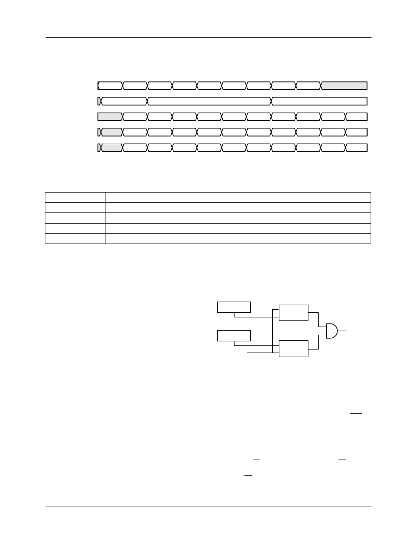
relation to the PD port. Control register OMIX chooses
among the following set of coefficients; either 0 1/8 1/2 7/8
1, 0 1/2 1 , or 0 1 to switch between the PD port and the over-
lay color. The timing diagram in Figure 22 identifies the
three possible output formats that the mixer can produce.
Figure 22. Overlay Outputs
Hardware Keying
The KEY input switches the input to the Comp2 data path
between the composite video generated from the PD port and
the CVBS data bus on a pixel-by-pixel basis. This is a “soft”
switch is executed over 3 PCK periods to minimize out-of-
band transients. Keying is accomplished in the digital com-
posite video domain. The coefficients for the mix are 0, 1/8,
1/2, 7/8, and 1 . The COMP2 output is the final output for all
overlay functions. The other three D/As will continue to
present PD port data when CVBS is active.
Hardware keying is enabled by the key Control Register
HKEN. Normally, keying is only effective during the active
video portion of the encoded video line (as determined by
Control Register VA). That is, the horizontal blanking inter-
val is generated by the encoder even if the KEY signal is
held HIGH through horizontal blanking. However, it is pos-
sible to allow digital horizontal blanking to be passed
through from the CVBS bus to the COMP2 output by setting
key Control Register BUKEN HIGH. In this mode, KEY is
always active, and may be exercised at will.
The KEY input is registered into the encoder just as Pixel
data is clocked into the PD port. It is internally pipelined, so
the midpoint of the KEY transition occurs at the output of
the pixel that was input at the same time at the KEY signal.
Data Keying
Data Keying occurs just prior to the gamma block. Data key-
ing for each channel Green/Y, Blue/C
b
, and Red/C
r
, is sepa-
rately enabled or disabled by the control registers
DKEYDIS, EKEYDIS, and FKEYDIS. On each channel the
eight (8) MSBs of the pixel data are compared against a
maximum key value and a minimum key value. If the pixel
data is greater than xKEYMIN and less than or equal to
xKEYMAX, then a key match is signaled for that channel.
Figure 23. Data Keying
By allowing a window of possible key values on each chan-
nel the TMC2193 opens a key cube in the color space.
Parallel Microprocessor Interface
The parallel microprocessor interface is active when SER is
HIGH and employs a 12-line interface; an 8 bit data bus and
2 bit address location, 1 bit read/write select, and a chip
select controlling the timing. Two addresses are required for
device programming, one to the pointer and one to the data
location. When writing, the address is presented along with a
LOW on the R/W pin during the falling edge of CS. Eight
bits of data are presented on D7-0 during the subsequent ris-
ing edge of CS.
Table 23. Overlay Address Map
OL4-0
0
1-15
16
17-31
Result
Pixel data is passed through overlay mixer.
Overlay is mixed with PD or CVBS at the transitions.
Half amplitude PD or half amplitude CVBS is the output of COMP2.
Overlay is mixed with half amplitude PD or half amplitude CVBS at the transitions.
A
A
>0
0
OL[4:0]
B
C
D
E
F
G
H
I
PDx
A
B
OL
OL
OL
I
OL
OL
H
A
B
1/2C, 1/2OL
OL
OL
I
OL
1/2G, 1/2OL
H
MixOUT (OMIX = 3)
A
7/8B, 1/8OL 1/2C, 1/2OL 1/8D, 7/8OL
OL
I
1/8F, 7/8OL 1/2G, 1/2OL 7/8H, 1/8OL
MixOUT (OMIX = 2)
MixOUT (OMIX = 1)
65-6294-24
xKEYMAX
A<=B
A
B
A<=B
A
B
KEY
MATCH
xKEYMIN
xCHANNEL
65-6294-25
相關(guān)PDF資料 |
PDF描述 |
|---|---|
| TMC2193 | 10 Bit Encoder |
| TMC22051AKHC | Circular Connector; No. of Contacts:11; Series:MS27484; Body Material:Aluminum; Connecting Termination:Crimp; Connector Shell Size:18; Circular Contact Gender:Pin; Circular Shell Style:Straight Plug; Insert Arrangement:18-11 RoHS Compliant: No |
| TMC22X5YA | Multistandard Digital Video Decoder Three-Line Adaptive Comb Decoder Family, 8 & 10 bit |
| TMC22052AKHC | Multistandard Digital Video Decoder Three-Line Adaptive Comb Decoder Family, 8 & 10 bit |
| TMC22053AKHC | Multistandard Digital Video Decoder Three-Line Adaptive Comb Decoder Family, 8 & 10 bit |
相關(guān)代理商/技術(shù)參數(shù) |
參數(shù)描述 |
|---|---|
| TMC22 WAF | 制造商:Fairchild Semiconductor Corporation 功能描述: |
| TMC22051 WAF | 制造商:Fairchild Semiconductor Corporation 功能描述: |
| TMC22051AKHC | 功能描述:多媒體雜項(xiàng) RoHS:否 制造商:Texas Instruments 類型: 通道數(shù)量: 轉(zhuǎn)換速率:540 Mbps 分辨率: 封裝 / 箱體:SOIC-16 封裝:Tube |
| TMC22052AKHC | 制造商:FAIRCHILD 制造商全稱:Fairchild Semiconductor 功能描述:Multistandard Digital Video Decoder Three-Line Adaptive Comb Decoder Family, 8 & 10 bit |
| TMC22053AKHC | 制造商:Rochester Electronics LLC 功能描述:- Bulk |
發(fā)布緊急采購,3分鐘左右您將得到回復(fù)。