- 您現(xiàn)在的位置:買(mǎi)賣(mài)IC網(wǎng) > PDF目錄383959 > TMC2193KJC (FAIRCHILD SEMICONDUCTOR CORP) 10 Bit Encoder PDF資料下載
參數(shù)資料
| 型號(hào): | TMC2193KJC |
| 廠(chǎng)商: | FAIRCHILD SEMICONDUCTOR CORP |
| 元件分類(lèi): | 消費(fèi)家電 |
| 英文描述: | 10 Bit Encoder |
| 中文描述: | SPECIALTY CONSUMER CIRCUIT, PQFP100 |
| 封裝: | MQFP-100 |
| 文件頁(yè)數(shù): | 28/72頁(yè) |
| 文件大小: | 448K |
| 代理商: | TMC2193KJC |
第1頁(yè)第2頁(yè)第3頁(yè)第4頁(yè)第5頁(yè)第6頁(yè)第7頁(yè)第8頁(yè)第9頁(yè)第10頁(yè)第11頁(yè)第12頁(yè)第13頁(yè)第14頁(yè)第15頁(yè)第16頁(yè)第17頁(yè)第18頁(yè)第19頁(yè)第20頁(yè)第21頁(yè)第22頁(yè)第23頁(yè)第24頁(yè)第25頁(yè)第26頁(yè)第27頁(yè)當(dāng)前第28頁(yè)第29頁(yè)第30頁(yè)第31頁(yè)第32頁(yè)第33頁(yè)第34頁(yè)第35頁(yè)第36頁(yè)第37頁(yè)第38頁(yè)第39頁(yè)第40頁(yè)第41頁(yè)第42頁(yè)第43頁(yè)第44頁(yè)第45頁(yè)第46頁(yè)第47頁(yè)第48頁(yè)第49頁(yè)第50頁(yè)第51頁(yè)第52頁(yè)第53頁(yè)第54頁(yè)第55頁(yè)第56頁(yè)第57頁(yè)第58頁(yè)第59頁(yè)第60頁(yè)第61頁(yè)第62頁(yè)第63頁(yè)第64頁(yè)第65頁(yè)第66頁(yè)第67頁(yè)第68頁(yè)第69頁(yè)第70頁(yè)第71頁(yè)第72頁(yè)
TMC2193
PRODUCT SPECIFICATION
28
REV. 1.0 3/26/03
Analog outputs of the TMC2193 are driven by four 10 bit
D/A converters and separate 9 bit reference D/A converter,
operating at twice the pixel rate. The outputs drive standard
video levels into 37.5 or 75 Ohm loads. An internal voltage
reference is used to provide reference current for the D/A
converters. For more accurate levels, an external fixed or
variable voltage reference source is accommodated. The
video signal levels from the TMC2193 may be adjusted by
varying the common Vref or the four independent Rrefs.
Each video D/A converter has an independent reference
resistor that can adjust the output gain, with the exception of
the reference D/A whose reference resistor is shared with
DAC1. D/A Matching is achieved by trimming the each
external reference resistor of each D/A.
Digital Composite Output
In addition, the TMC2193 supplies a 10 bit digital composite
signal on pins D[7:0] and FLD[2:1]. The digital composite
output can be either an interpolated signal on a non-interpo-
lated signal, this controlled by the control register
SEL_CLK.
Ancillary Data
Control Registers for this section
The TMC2193 is designed to accept 15 words of ancillary
data after the active video pixels at the end of each horizontal
line. Ancillary data may occur once per line, once per field,
once per eight fields, on random lines, or not al all. The
TMC2193 does not assume ancillary data is present on a reg-
ular basis.
Note:
1. P = odd parity bit, x = reserved bit will be ignored
The first three words of ancillary data comprise the TRS sig-
nal (ANC2-0) which indicates the end of active video. Also
known as the Ancillary data header, the TRS signal is a 00
h
,
FF
h
, FF
h
sequence. Except for the TRS words, ancillary data
bit 0 (B
0
, LSB) is odd parity for B
7-1
.
The data type word (TT) is used to specify the ancillary data
type. The TMC2193 compares this 7 bit value with the con-
tents of the ANCID control register. If there is a match, the
ancillary data will be processed. If there is no match, the
TMC2193 ignores ancillary data.
The word count data (D
11-0
in MM, LL) in the ancillary data
packet indicate the number of words in ancillary data.
Ancillary phase data is used to program the MSBs of the
PHASE register. ANCPHEN and PHV determine how ancil-
lary phase data is used. When ancillary data is not present,
the TMC2193 assumes PHV = LOW.
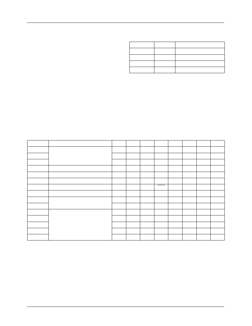
Address
0x07
0x07
0x07
0x08
Bit(s)
2
1
0
7-0
Name
ANCFREN
ANCPHEN
ANCTREN
ANCID
Table 18. Ancillary Data Format
Word ID
ANC2
ANC1
ANC0
TT
MM
LL
FIELD
Description
Ancillary Data Header (Timing
Reference Signal)
B
7
0
1
1
TT6
0
0
x
x
PHV
PH
6
FRV
FR
27
FR
20
FR
13
FR
6
B
6
0
1
1
TT5
D11
D5
x
x
PH
12
PH
5
x
FR
26
FR
19
FR
12
FR
5
B
5
0
1
1
TT4
D10
D4
x
x
PH
11
PH
4
x
FR
25
FR
18
FR
11
FR
4
B
4
0
1
1
TT3
D9
D3
SVF
x
PH
10
PH
3
FR
31
FR
24
FR
17
FR
10
FR
3
B
3
0
1
1
TT2
D8
D2
F2
x
PH
9
PH
2
FR
30
FR
23
FR
16
FR
9
FR
2
B
2
0
1
1
TT1
D7
D1
F1
x
PH
8
PH
1
FR
29
FR
22
FR
15
FR
8
FR
1
B
1
0
1
1
TT0
D6
D0
F0
x
PH
7
PH
0
FR
28
FR
21
FR
14
FR
7
FR
0
B
0
0
1
1
P
P
P
P
P
P
P
P
P
P
P
P
Data Type
Word
Count
Field ID/Synchronous Video Flag
reserved
Subcarrier Phase
PH1
PH0
FR4
FR3
FR2
FR1
FR0
Subcarrier Frequency
相關(guān)PDF資料 |
PDF描述 |
|---|---|
| TMC2193 | 10 Bit Encoder |
| TMC22051AKHC | Circular Connector; No. of Contacts:11; Series:MS27484; Body Material:Aluminum; Connecting Termination:Crimp; Connector Shell Size:18; Circular Contact Gender:Pin; Circular Shell Style:Straight Plug; Insert Arrangement:18-11 RoHS Compliant: No |
| TMC22X5YA | Multistandard Digital Video Decoder Three-Line Adaptive Comb Decoder Family, 8 & 10 bit |
| TMC22052AKHC | Multistandard Digital Video Decoder Three-Line Adaptive Comb Decoder Family, 8 & 10 bit |
| TMC22053AKHC | Multistandard Digital Video Decoder Three-Line Adaptive Comb Decoder Family, 8 & 10 bit |
相關(guān)代理商/技術(shù)參數(shù) |
參數(shù)描述 |
|---|---|
| TMC22 WAF | 制造商:Fairchild Semiconductor Corporation 功能描述: |
| TMC22051 WAF | 制造商:Fairchild Semiconductor Corporation 功能描述: |
| TMC22051AKHC | 功能描述:多媒體雜項(xiàng) RoHS:否 制造商:Texas Instruments 類(lèi)型: 通道數(shù)量: 轉(zhuǎn)換速率:540 Mbps 分辨率: 封裝 / 箱體:SOIC-16 封裝:Tube |
| TMC22052AKHC | 制造商:FAIRCHILD 制造商全稱(chēng):Fairchild Semiconductor 功能描述:Multistandard Digital Video Decoder Three-Line Adaptive Comb Decoder Family, 8 & 10 bit |
| TMC22053AKHC | 制造商:Rochester Electronics LLC 功能描述:- Bulk |
發(fā)布緊急采購(gòu),3分鐘左右您將得到回復(fù)。