- 您現(xiàn)在的位置:買賣IC網(wǎng) > PDF目錄383876 > T7688 (Lineage Power) 5.0 V E1/CEPT Quad Line Interface(5.0 V E1/CEPT四線接口) PDF資料下載
參數(shù)資料
| 型號(hào): | T7688 |
| 廠商: | Lineage Power |
| 英文描述: | 5.0 V E1/CEPT Quad Line Interface(5.0 V E1/CEPT四線接口) |
| 中文描述: | 5.0V的E1/CEPT四線接口(5.0V的E1/CEPT四線接口) |
| 文件頁數(shù): | 8/38頁 |
| 文件大小: | 577K |
| 代理商: | T7688 |
第1頁第2頁第3頁第4頁第5頁第6頁第7頁當(dāng)前第8頁第9頁第10頁第11頁第12頁第13頁第14頁第15頁第16頁第17頁第18頁第19頁第20頁第21頁第22頁第23頁第24頁第25頁第26頁第27頁第28頁第29頁第30頁第31頁第32頁第33頁第34頁第35頁第36頁第37頁第38頁
Data Sheet
May 1998
T7688 5.0 V E1/CEPT Quad Line Interface
8
Lucent Technologies Inc.
25
INT
O
Interrupt
. This pin is asserted high to indicate an interrupt produced by an
alarm condition in register 0 or 1. The activation of this pin can be masked
by microprocessor registers 2, 3, and 4.
26
RDY_DTACK
O
Ready
. If MPMODE = 1 (pin 21), this pin is asserted high to indicate the
device has completed a read or write operation. This pin is in a 3-state con-
dition when CS (pin 24) is high.
Data Transfer Acknowledge (Active-Low).
If MPMODE = 0 (pin 21), this
pin is asserted low to indicate the device has completed a read or write
operation.
27, 78
GND
C
P
Ground Reference for Microprocessor Interface and Control Circuitry
.
28, 77
V
DDC
P
Power Supply for Microprocessor Interface and Control Circuitry.
The
T7688 device requires a 5 V
±
5% power supply on these pins.
Reference Clock
. A valid reference clock (32.768 MHz
±
100 ppm for CEPT
operation) must be provided at this input for certain applications (see the
XCLK Reference Clock section). XCLK must be an independent, continu-
ously active, ungapped, and unjittered clock to guarantee device perfor-
mance specifications. An internal 100 k
pull-up is on this pin.
Blue Clock
. Input clock signal used to transmit the blue signal (all 1s data
pattern). In CEPT mode, this clock is 2.048 MHz
±
50 ppm. An internal
100 k
pull-up is on this pin.
Loss of XCLK
.
This pin is asserted high when the XCLK signal (pin 29) is
not present.
29
XCLK
I
u
30
BCLK
I
u
31
LOXC
O
32
RESET
I
u
Hardware Reset (Active-Low)
. If
RESET
is forced low, all internal states in
the line interface paths are reset and data flow through each channel will be
momentarily disrupted (see the RESET (RESET, SWRESET) section). The
RESET
pin must be held low for a minimum of 10
μ
s. An internal 50 k
pull-
up is on this pin.
33
ICT
I
u
In-Circuit Test Control (Active-Low)
. If
ICT
is forced low, certain output
pins are placed in a high-impedance state (see the In-Circuit Testing and
Driver 3-state (ICT) section). An internal 50 k
pull-up is on this pin.
Microprocessor Interface Address/Data Bus.
If MPMUX = 0 (pin 20),
these pins become the bidirectional, 3-statable data bus. If MPMUX = 1,
these pins become the multiplexed address/data bus. In this mode, only the
lower 4 bits (AD[3:0]) are used for the internal register addresses.
69
AD7
I/O
70
AD6
71
AD5
72
AD4
73
AD3
74
AD2
75
AD1
76
AD0
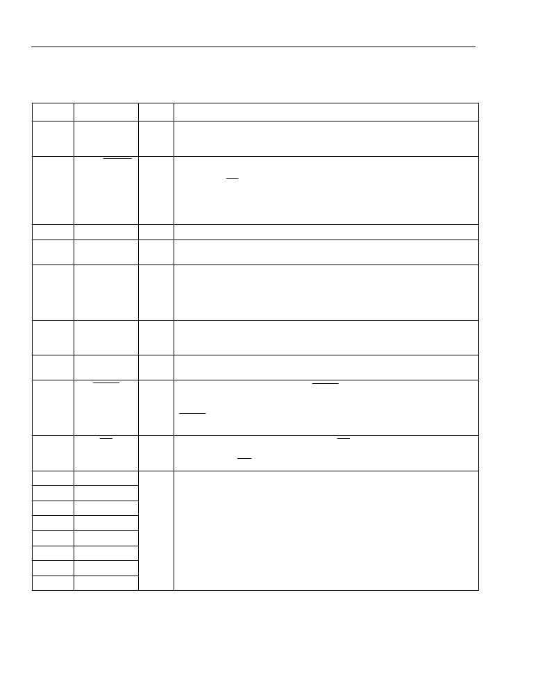
Table 1. Pin Descriptions
(continued)
Pin
Symbol
Type
*
Name/Description
* P = power, I = input, O = output, and I
u
= input with internal pull-up.
Pin Information
(continued)
相關(guān)PDF資料 |
PDF描述 |
|---|---|
| T7689 | 5.0 V T1 Quad Line Interface(5.0 V T1四線接口) |
| T7690 | 5.0 V T1/E1 Quad Line Interface(5.0 V T1/E1 四線接口) |
| T7693 | 3.3 V T1/E1 Quad Line Interface( 3.3 V T1/E四線接口) |
| T7698 | Quad T1/E1 Line Interface and Octal T1/E1 Monitor(四T1/E1線接口和八T1/E1監(jiān)控器) |
| T7705A | SUPPLY-VOLTAGE SUPERVISORS |
相關(guān)代理商/技術(shù)參數(shù) |
參數(shù)描述 |
|---|---|
| T-7689-FL | 制造商:Alcatel-Lucent 功能描述:DATACOM, PCM TRANSCEIVER, 100 Pin Plastic QFP |
| T-7689---FL-DB | 制造商:Rochester Electronics LLC 功能描述:- Bulk 制造商:LSI Corporation 功能描述: |
| T-7690-FL | 制造商:Alcatel-Lucent 功能描述:PCM TRANSCEIVER, Quad, CEPT PCM-30/E-1, 100 Pin, Plastic, QFP |
| T77 | 制造商:Thomas & Betts 功能描述:2-1/2"CONDUIT BODY,IRON,T,F-7 制造商:Cooper Crouse-Hinds 功能描述: 制造商:Thomas & Betts 功能描述:Fittings T-Fitting 2.5inch Non-Thread Iron |
| T7700 | 制造商:INTEL 制造商全稱:Intel Corporation 功能描述:Core2 Duo Processors and Core2 Extreme Processors for Platforms Based on Mobile 965 Express Chipset Family |
發(fā)布緊急采購,3分鐘左右您將得到回復(fù)。