- 您現(xiàn)在的位置:買(mǎi)賣(mài)IC網(wǎng) > PDF目錄383876 > T7688 (Lineage Power) 5.0 V E1/CEPT Quad Line Interface(5.0 V E1/CEPT四線接口) PDF資料下載
參數(shù)資料
| 型號(hào): | T7688 |
| 廠商: | Lineage Power |
| 英文描述: | 5.0 V E1/CEPT Quad Line Interface(5.0 V E1/CEPT四線接口) |
| 中文描述: | 5.0V的E1/CEPT四線接口(5.0V的E1/CEPT四線接口) |
| 文件頁(yè)數(shù): | 21/38頁(yè) |
| 文件大小: | 577K |
| 代理商: | T7688 |
第1頁(yè)第2頁(yè)第3頁(yè)第4頁(yè)第5頁(yè)第6頁(yè)第7頁(yè)第8頁(yè)第9頁(yè)第10頁(yè)第11頁(yè)第12頁(yè)第13頁(yè)第14頁(yè)第15頁(yè)第16頁(yè)第17頁(yè)第18頁(yè)第19頁(yè)第20頁(yè)當(dāng)前第21頁(yè)第22頁(yè)第23頁(yè)第24頁(yè)第25頁(yè)第26頁(yè)第27頁(yè)第28頁(yè)第29頁(yè)第30頁(yè)第31頁(yè)第32頁(yè)第33頁(yè)第34頁(yè)第35頁(yè)第36頁(yè)第37頁(yè)第38頁(yè)
Data Sheet
May 1998
T7688 5.0 V E1/CEPT Quad Line Interface
21
Lucent Technologies Inc.
Microprocessor Interface
(continued)
Microprocessor Clock (MPCLK) Specifications
The microprocessor interface is designed to operate at clock speeds up to 16.384 MHz without requiring any wait-
states. Wait-states may be needed if higher microprocessor clock speeds are required. The microprocessor clock
(MPCLK, pin 83) specification is shown in Table 10. This clock must be supplied only if the RDY_DTACK and INT
outputs are required to be synchronous to MPCLK. Otherwise, the MPCLK pin must be connected to ground
(GND
D
).
Internal Chip Select Function
When the microprocessor interface is configured to operate in the multiplexed address/data bus modes (MPUX =
1), the user has access to an internal chip select function. This function allows a microprocessor to selectively read
or write a specific quad line interface device in a system of up to eight devices on the microprocessor bus. Exter-
nally tying CS = 0 (pin 24) and A3 = 1 (pin 79) on every line interface device enables the internal chip select func-
tion. Individual device addresses are established by externally connecting the other three address pins A[2:0] to a
unique address value in the range of 000 through 111. In order for a line interface device to respond to the register
read or write request from the microprocessor, the address data bus AD[6:4] (pins 70, 71, 72) must match the spe-
cific address defined on A[2:0]. If
CS
and A3 pins are tied low, the internal chip select function is disabled and all
line interface devices will respond to a microprocessor write request. However, if
CS
= 1, none of the line interface
devices will respond to the microprocessor read/write request.
Microprocessor Interface Register Architecture
The register bank architecture of the microprocessor interface is shown in Table 11. The register bank consists of
sixteen 8-bit registers classified as alarm registers, global control registers, and channel configuration/mainte-
nance registers. Registers 0 and 1 are the alarm registers used for storing the various device alarm status and are
read-only. All other registers are read/write. Registers 2 and 3 contain the individual mask bits for the alarms in reg-
isters 0 and 1. Registers 4 and 5 are designated as the global control registers used to set up the functions for all
four channels. The channel configuration registers in registers 6 through 9 are used to configure the individual
channel functions and parameters. Registers 10 and 11 must be cleared by the user after a powerup for proper
device operation. Registers 12 through 15 are reserved for proprietary functions and must not be addressed during
operation. The following sections describe these registers in detail.
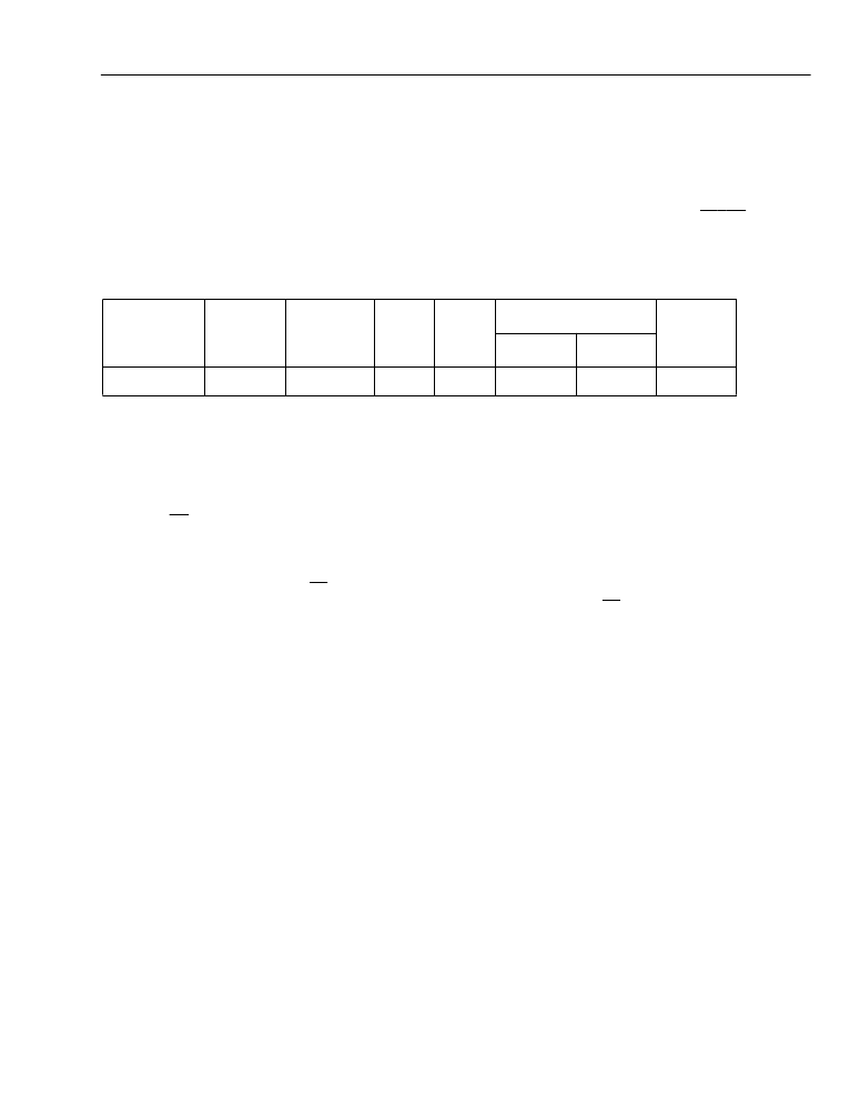
Table 10. Microprocessor Input Clock Specifications
Name
Symbol
Period and
Tolerance
T
rise
Typ
T
fall
Typ
Duty Cycle
Unit
Min High
Min Low
MPCLK
t1
61 to 323
5
5
27
27
ns
相關(guān)PDF資料 |
PDF描述 |
|---|---|
| T7689 | 5.0 V T1 Quad Line Interface(5.0 V T1四線接口) |
| T7690 | 5.0 V T1/E1 Quad Line Interface(5.0 V T1/E1 四線接口) |
| T7693 | 3.3 V T1/E1 Quad Line Interface( 3.3 V T1/E四線接口) |
| T7698 | Quad T1/E1 Line Interface and Octal T1/E1 Monitor(四T1/E1線接口和八T1/E1監(jiān)控器) |
| T7705A | SUPPLY-VOLTAGE SUPERVISORS |
相關(guān)代理商/技術(shù)參數(shù) |
參數(shù)描述 |
|---|---|
| T-7689-FL | 制造商:Alcatel-Lucent 功能描述:DATACOM, PCM TRANSCEIVER, 100 Pin Plastic QFP |
| T-7689---FL-DB | 制造商:Rochester Electronics LLC 功能描述:- Bulk 制造商:LSI Corporation 功能描述: |
| T-7690-FL | 制造商:Alcatel-Lucent 功能描述:PCM TRANSCEIVER, Quad, CEPT PCM-30/E-1, 100 Pin, Plastic, QFP |
| T77 | 制造商:Thomas & Betts 功能描述:2-1/2"CONDUIT BODY,IRON,T,F-7 制造商:Cooper Crouse-Hinds 功能描述: 制造商:Thomas & Betts 功能描述:Fittings T-Fitting 2.5inch Non-Thread Iron |
| T7700 | 制造商:INTEL 制造商全稱(chēng):Intel Corporation 功能描述:Core2 Duo Processors and Core2 Extreme Processors for Platforms Based on Mobile 965 Express Chipset Family |
發(fā)布緊急采購(gòu),3分鐘左右您將得到回復(fù)。