- 您現(xiàn)在的位置:買賣IC網(wǎng) > PDF目錄383840 > ST92R195C ROMLESS HCMOS MCU WITH ON-SCREEN-DISPLAY AND TELETEXT DATA SLICER PDF資料下載
參數(shù)資料
| 型號(hào): | ST92R195C |
| 英文描述: | ROMLESS HCMOS MCU WITH ON-SCREEN-DISPLAY AND TELETEXT DATA SLICER |
| 中文描述: | 無ROM HCMOS微控制器屏幕顯示和圖文電視數(shù)據(jù)限幅器 |
| 文件頁數(shù): | 61/208頁 |
| 文件大小: | 2312K |
| 代理商: | ST92R195C |
第1頁第2頁第3頁第4頁第5頁第6頁第7頁第8頁第9頁第10頁第11頁第12頁第13頁第14頁第15頁第16頁第17頁第18頁第19頁第20頁第21頁第22頁第23頁第24頁第25頁第26頁第27頁第28頁第29頁第30頁第31頁第32頁第33頁第34頁第35頁第36頁第37頁第38頁第39頁第40頁第41頁第42頁第43頁第44頁第45頁第46頁第47頁第48頁第49頁第50頁第51頁第52頁第53頁第54頁第55頁第56頁第57頁第58頁第59頁第60頁當(dāng)前第61頁第62頁第63頁第64頁第65頁第66頁第67頁第68頁第69頁第70頁第71頁第72頁第73頁第74頁第75頁第76頁第77頁第78頁第79頁第80頁第81頁第82頁第83頁第84頁第85頁第86頁第87頁第88頁第89頁第90頁第91頁第92頁第93頁第94頁第95頁第96頁第97頁第98頁第99頁第100頁第101頁第102頁第103頁第104頁第105頁第106頁第107頁第108頁第109頁第110頁第111頁第112頁第113頁第114頁第115頁第116頁第117頁第118頁第119頁第120頁第121頁第122頁第123頁第124頁第125頁第126頁第127頁第128頁第129頁第130頁第131頁第132頁第133頁第134頁第135頁第136頁第137頁第138頁第139頁第140頁第141頁第142頁第143頁第144頁第145頁第146頁第147頁第148頁第149頁第150頁第151頁第152頁第153頁第154頁第155頁第156頁第157頁第158頁第159頁第160頁第161頁第162頁第163頁第164頁第165頁第166頁第167頁第168頁第169頁第170頁第171頁第172頁第173頁第174頁第175頁第176頁第177頁第178頁第179頁第180頁第181頁第182頁第183頁第184頁第185頁第186頁第187頁第188頁第189頁第190頁第191頁第192頁第193頁第194頁第195頁第196頁第197頁第198頁第199頁第200頁第201頁第202頁第203頁第204頁第205頁第206頁第207頁第208頁
61/208
ST92R195C - RESET AND CLOCK CONTROL UNIT (RCCU)
OSCILLATOR CHARACTERISTICS
(Cont’d)
The following table is relative to the fundamental
quartz crystal only; assuming:
– Rs: parasitic series resistance of the quartz crys-
tal (upper limit)
– C0: parasitic capacitance of the crystal (upper
limit,
≤
7 pF)
– C1,C2: maximum total capacitance on pins OS-
CIN/OSCOUT (value including external capaci-
tance tied to the pin plus the parasitic
capacitance of the board and device).
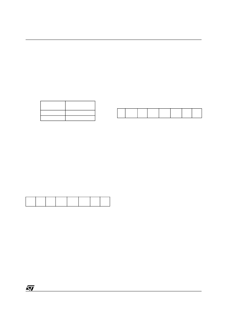
Table 9. Crystal Specification (C0
≤
7 pF)
Legend
:
Rs: Parasitic Series Resistance of the quartz crystal (up-
per limit) C0: Parasitic capacitance of the quartz crystal
(upper limit, < 7pF)
C1, C2: Maximum Total Capacitance on pins OSCIN and
OSCOUT (the value includes the external capacitance
tied to the pin plus the parasitic capacitance of the board
and of the device)
gm: Transconductance of the oscillator
Note
.The tables are relative to the fundamental quartz
crystal only (not ceramic resonator).
5.4 CLOCK CONTROL REGISTERS
MODE REGISTER (MODER)
R235 - Read/Write
Register Group: E (System)
Reset Value: 1110 0000 (E0h)
Bit 7:6 = Bits described in Device Architecture
chapter.
Bit 5 =
DIV2
:
OSCIN Divided by 2
.
This bit controls the divide by 2 circuit which oper-
ates on the OSCIN Clock.
0: No division of OSCIN Clock
1: OSCIN clock is internally divided by 2
Bit 4:2 =
PRS[2:0]
:
Clock
Prescaling
.
These bits define the prescaler value used to
prescale CPUCLK from INTCLK. When they are
reset, the CPUCLK is not prescaled, and is equal
to INTCLK; in all other cases, the internal clock is
prescaled by the value of these three bits plus one.
Bit 1:0 = Bits described in Device Architecture
chapter.
WAIT CONTROL REGISTER
(
WCR)
R252
-
Read/Write
Register Page: 0
Reset Value: 0111 1111 (7Fh)
Bit 7 = Reserved, read as “0”.
Bit 6 =
WDGEN
: refer to Timer/Watchdog chapter.
WARNING. Resetting this bit to zero has the effect
of setting the Timer/Watchdog to the Watchdog
mode. Unless this is desired, this must be set to
“1”.
Bit 5:3 =
WDM[2:0]
:
Data Memory Wait Cycles.
These bits contain the number of INTCLK cycles
to be added automatically to external Data memo-
ry accesses. WDM = 0 gives no additional wait cy-
cles. WDM = 7 provides the maximum 7 INTCLK
cycles (reset condition).
Bit 2:0 =
WPM[2:0]
:
Program Memory Wait Cy-
cles.
These bits contain the number of INTCLK cycles
to be added automatically to external Program
memory accesses. WPM = 0 gives no additional
wait cycles, WPM = 7 provides the maximum 7
INTCLK cycles (reset condition).
Note:
The number of clock cycles added refers to
INTCLK and NOT to CPUCLK.
WARNING.
The reset value of the Wait Control
Register gives the maximum number of Wait cy-
cles for external memory. To get optimum per-
formance from the ST9 when used in single-chip
mode (no external memory) the user should write
the WDM2,1,0 and WPM2,1,0 bits to “0”.
Frequency
C1 = C2 = 39 pF
Rs Max
65
260
8
4
7
0
1
1
DIV2
PRS2
PRS1
PRS0
0
0
7
0
0
WDGEN WDM2 WDM1
WDM0
WPM2 WPM1 WPM0
相關(guān)PDF資料 |
PDF描述 |
|---|---|
| STA003 | MPEG 2.5 LAYER III AUDIO DECODER |
| STA10 | ASIC |
| STA351A | General Purpose Sink Driver Array |
| STA352A | General Purpose Source Driver Array |
| STA474A | H-bridge Motor Driver Array |
相關(guān)代理商/技術(shù)參數(shù) |
參數(shù)描述 |
|---|---|
| ST92T141K4B6 | 功能描述:8位微控制器 -MCU OTP EPROM 16K SPI RoHS:否 制造商:Silicon Labs 核心:8051 處理器系列:C8051F39x 數(shù)據(jù)總線寬度:8 bit 最大時(shí)鐘頻率:50 MHz 程序存儲(chǔ)器大小:16 KB 數(shù)據(jù) RAM 大小:1 KB 片上 ADC:Yes 工作電源電壓:1.8 V to 3.6 V 工作溫度范圍:- 40 C to + 105 C 封裝 / 箱體:QFN-20 安裝風(fēng)格:SMD/SMT |
| ST92T141K4M6 | 功能描述:8位微控制器 -MCU OTP EPROM 16K SPI RoHS:否 制造商:Silicon Labs 核心:8051 處理器系列:C8051F39x 數(shù)據(jù)總線寬度:8 bit 最大時(shí)鐘頻率:50 MHz 程序存儲(chǔ)器大小:16 KB 數(shù)據(jù) RAM 大小:1 KB 片上 ADC:Yes 工作電源電壓:1.8 V to 3.6 V 工作溫度范圍:- 40 C to + 105 C 封裝 / 箱體:QFN-20 安裝風(fēng)格:SMD/SMT |
| ST92T163R4T1 | 功能描述:8位微控制器 -MCU OTP EPROM 20K USB/I2 RoHS:否 制造商:Silicon Labs 核心:8051 處理器系列:C8051F39x 數(shù)據(jù)總線寬度:8 bit 最大時(shí)鐘頻率:50 MHz 程序存儲(chǔ)器大小:16 KB 數(shù)據(jù) RAM 大小:1 KB 片上 ADC:Yes 工作電源電壓:1.8 V to 3.6 V 工作溫度范圍:- 40 C to + 105 C 封裝 / 箱體:QFN-20 安裝風(fēng)格:SMD/SMT |
| ST92T196/JAP | 制造商:STMicroelectronics 功能描述: |
| ST92T96N9B1/AIN | 制造商:STMicroelectronics 功能描述: |
發(fā)布緊急采購,3分鐘左右您將得到回復(fù)。