- 您現(xiàn)在的位置:買賣IC網(wǎng) > PDF目錄383804 > SAA7708H (NXP Semiconductors N.V.) Car Radio Digital Signal Processor PDF資料下載
參數(shù)資料
| 型號(hào): | SAA7708H |
| 廠商: | NXP Semiconductors N.V. |
| 元件分類: | 數(shù)字信號(hào)處理 |
| 英文描述: | Car Radio Digital Signal Processor |
| 中文描述: | 汽車無(wú)線電數(shù)字信號(hào)處理器 |
| 文件頁(yè)數(shù): | 49/60頁(yè) |
| 文件大小: | 281K |
| 代理商: | SAA7708H |
第1頁(yè)第2頁(yè)第3頁(yè)第4頁(yè)第5頁(yè)第6頁(yè)第7頁(yè)第8頁(yè)第9頁(yè)第10頁(yè)第11頁(yè)第12頁(yè)第13頁(yè)第14頁(yè)第15頁(yè)第16頁(yè)第17頁(yè)第18頁(yè)第19頁(yè)第20頁(yè)第21頁(yè)第22頁(yè)第23頁(yè)第24頁(yè)第25頁(yè)第26頁(yè)第27頁(yè)第28頁(yè)第29頁(yè)第30頁(yè)第31頁(yè)第32頁(yè)第33頁(yè)第34頁(yè)第35頁(yè)第36頁(yè)第37頁(yè)第38頁(yè)第39頁(yè)第40頁(yè)第41頁(yè)第42頁(yè)第43頁(yè)第44頁(yè)第45頁(yè)第46頁(yè)第47頁(yè)第48頁(yè)當(dāng)前第49頁(yè)第50頁(yè)第51頁(yè)第52頁(yè)第53頁(yè)第54頁(yè)第55頁(yè)第56頁(yè)第57頁(yè)第58頁(yè)第59頁(yè)第60頁(yè)
1998 May 19
49
Philips Semiconductors
Preliminary specification
Car Radio Digital Signal Processor
SAA7708H
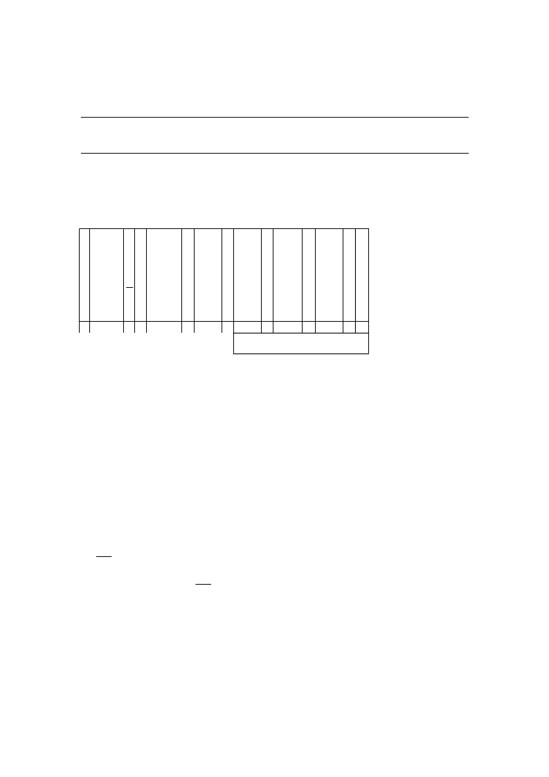
20.3
CDSP write cycles
The I
2
C bus configuration for a WRITE cycle is shown in table Table 16. The write cycle is used to write the bytes to
control the DCS block, the PLL for the DSP clock generation, the IAC settings, the AD volume control settings, the analog
input selection, the format of the I
2
S and some other settings. More detail can be found in the I
2
C memory map, Table 19.
Table 16
Master transmitter writes to the CDSP registers.
The datalength is 2 bytes or 3 bytes depending of the accessed memory. If the Y-memory is addressed the data length
is 2 bytes, in case of the X-memory the length is 3 bytes. The slave receiver detects the address and adjusts the number
of bytes accordingly.
20.4
CDSP READ cycles
The I
2
C bus configuration for a read cycle is shown in table Table 17. The read cycle is used to read the data values from
XRAM or YRAM. The master starts with a start condition S, the CDSP address ‘0011100’ and a ‘0’ (Write) for the
read/write bit. This is followed by an acknowledge by the CDSP. Then the Master writes the memory address High and
memory addres Low where the reading of the memory content of the CDSP must start. The CDSP acknowledges these
addresses both. Then the master generates a repeated Start (Sr) and again the CDSP address ‘0011100’ but this time
followed by a ‘1’ (Read) of the read/write bit. From this moment on the CDSP will sent the memory content in groups of
2 (Y-memory) or 3 (X-memory) bytes to the I
2
C bus each time acknowledged by the Master. The Master stops this cycle
by generating a Negative Acknowledge, then the CDSP frees the I
2
C bus and the Master can generate a Stop condition.
The data is transferred from the DSP register to the I
2
C register at execution of the MPI instruction in the DSP program.
R
/
W
A
C
K
N
.
C
D
S
P
A
C
K
N
.
C
D
S
P
A
C
K
N
.
C
D
S
P
A
C
K
N
.
C
D
S
P
A
C
K
N.
C
D
S
P
A
C
K
N
.
C
D
S
P
S 0011100 0
A
AddrH
A
AddrL
A DataH
auto increment if repeated n-groups of
3 (2) bytes
A
DataM
A
DataL
A
P
S
P
A
AddrH and AddrL
DataH, DataM and DataL
DataH and DataM
= Start condition
= Stop condition
= Acknowledge from CDSP
= Address DSP register
= Data of XRAM or registers
= Data of YRAM
相關(guān)PDF資料 |
PDF描述 |
|---|---|
| SAL175UF-A | HERMETIC ULTRAFAST DIODE |
| SAL200UF-A | HERMETIC ULTRAFAST DIODE |
| SAL225UF-A | HERMETIC ULTRAFAST DIODE |
| SAL250UF-A | HERMETIC ULTRAFAST DIODE |
| SAL175UF3A | HERMETIC ULTRAFAST DIODE |
相關(guān)代理商/技術(shù)參數(shù) |
參數(shù)描述 |
|---|---|
| SAA7709/N107 | 制造商:PHILIPS-SEMI 功能描述: |
| SAA7709H/N103 | 功能描述:音頻 DSP DIGITAL SIGNAL PROCESSOR RoHS:否 制造商:Texas Instruments 工作電源電壓: 電源電流: 工作溫度范圍: 安裝風(fēng)格: 封裝 / 箱體: 封裝:Tube |
| SAA7709H/N103,518 | 功能描述:音頻 DSP DIRAC-2 RoHS:否 制造商:Texas Instruments 工作電源電壓: 電源電流: 工作溫度范圍: 安裝風(fēng)格: 封裝 / 箱體: 封裝:Tube |
| SAA7709H/N103,557 | 功能描述:音頻 DSP DIGITAL SIGNAL RoHS:否 制造商:Texas Instruments 工作電源電壓: 電源電流: 工作溫度范圍: 安裝風(fēng)格: 封裝 / 箱體: 封裝:Tube |
| SAA7709H/N103/S420 | 功能描述:音頻 DSP Car radio Digital Signal Processor RoHS:否 制造商:Texas Instruments 工作電源電壓: 電源電流: 工作溫度范圍: 安裝風(fēng)格: 封裝 / 箱體: 封裝:Tube |
發(fā)布緊急采購(gòu),3分鐘左右您將得到回復(fù)。