- 您現(xiàn)在的位置:買賣IC網(wǎng) > PDF目錄367854 > PDI1394L41 (NXP Semiconductors N.V.) Content Protection AV Link Layer(內(nèi)容可保護(hù)的AV鏈接層控制器) PDF資料下載
參數(shù)資料
| 型號(hào): | PDI1394L41 |
| 廠商: | NXP Semiconductors N.V. |
| 英文描述: | Content Protection AV Link Layer(內(nèi)容可保護(hù)的AV鏈接層控制器) |
| 中文描述: | 影音內(nèi)容保護(hù)鏈路層(內(nèi)容可保護(hù)的視聽(tīng)鏈接層控制器) |
| 文件頁(yè)數(shù): | 16/81頁(yè) |
| 文件大?。?/td> | 303K |
| 代理商: | PDI1394L41 |
第1頁(yè)第2頁(yè)第3頁(yè)第4頁(yè)第5頁(yè)第6頁(yè)第7頁(yè)第8頁(yè)第9頁(yè)第10頁(yè)第11頁(yè)第12頁(yè)第13頁(yè)第14頁(yè)第15頁(yè)當(dāng)前第16頁(yè)第17頁(yè)第18頁(yè)第19頁(yè)第20頁(yè)第21頁(yè)第22頁(yè)第23頁(yè)第24頁(yè)第25頁(yè)第26頁(yè)第27頁(yè)第28頁(yè)第29頁(yè)第30頁(yè)第31頁(yè)第32頁(yè)第33頁(yè)第34頁(yè)第35頁(yè)第36頁(yè)第37頁(yè)第38頁(yè)第39頁(yè)第40頁(yè)第41頁(yè)第42頁(yè)第43頁(yè)第44頁(yè)第45頁(yè)第46頁(yè)第47頁(yè)第48頁(yè)第49頁(yè)第50頁(yè)第51頁(yè)第52頁(yè)第53頁(yè)第54頁(yè)第55頁(yè)第56頁(yè)第57頁(yè)第58頁(yè)第59頁(yè)第60頁(yè)第61頁(yè)第62頁(yè)第63頁(yè)第64頁(yè)第65頁(yè)第66頁(yè)第67頁(yè)第68頁(yè)第69頁(yè)第70頁(yè)第71頁(yè)第72頁(yè)第73頁(yè)第74頁(yè)第75頁(yè)第76頁(yè)第77頁(yè)第78頁(yè)第79頁(yè)第80頁(yè)第81頁(yè)

Philips Semiconductors
Preliminary specification
PDI1394L41
1394 content protection AV link layer controller
2000 Apr 15
13
12.3.2
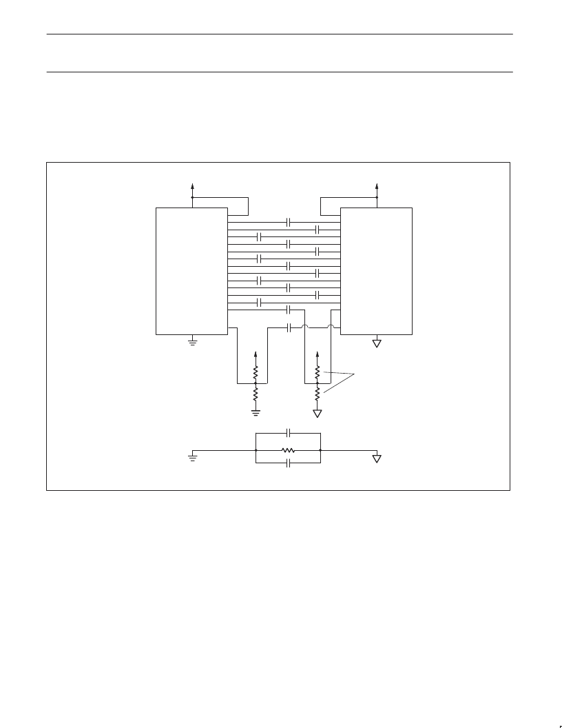
The circuit example (Figure 3) shows the connections required to implement basic single capacitor Link/PHY isolation.
Single capacitor isolation
NOTE:
The isolation enablement pins on both devices are in their “1” states, activating the bushold circuits on each part. The bushold circuits
provide local dc ground references to each side of the isolating/coupling capacitors. Also note that ground isolation/signal-coupling must be
provided in the form of a parallel combination of resistance and capacitance as indicated in the IEEE 1394 standard.
ISO–
SYSCLK
D0
D1
D2
D3
D4
D5
D6
D7
PHYCTL0
PHYCTL1
LREQ
LPS
PHY
PDI1394P2x
C
r
C
c
1MEG
ISON
SCLK
PHY D0
PHY D1
PHY D2
PHY D3
PHY D4
PHY D5
PHY D6
PHY D7
PHYCTL0
PHYCTL1
LREQ
LINK
PDI1394L41
APPLICATION/LINK
+3.3V
ISOLATED/PHY
+3.3V
SV01816
C
C
= 1 nF; C
r
= 100 nF; C
L
= 3.3nF
LPS
LINKON
APPLICATION AND LINK GROUND
ISOLATED PHY GROUND
LINKON
C
L
LINK
3.3V
PHY
3.3V
C
L
VALUES OF THESE RESISTORS DEPEND
ON PHY USED. SEE PHY DATASHEET.
C
c
13K
9.1K
C
c
C
c
C
c
C
c
C
c
C
c
C
c
C
c
C
c
C
c
C
c
ALSO SEE APPLICATION NOTE AN2452
FOR MORE DETAILS
Figure 3.
Single capacitor Link/PHY isolation
12.4
The PDI1394L41 implements several features for power management as noted in the P1394a draft 5.0 These features include:
Power Management
1. Reset of the Phy/Link interface by setting the RPL bit in the LNKCTL register.
2. Disable of the Phy/Link interface caused by either setting the SWPD bit in the RDI register –OR– asserting (high) the PD pin.
3. Initialization of the Phy/Link interface after it was disabled or reset.
The application can power up the Phy/Link interface by deasserting the PD pin –OR– clearing (low) the SWPD in the RDI register. This will
cause the L41 to produce a pulsing signal on the LPS pin. When the L41 is in power down mode, reads and writes to the host interface will be
restricted to those addressing only the RDI register (0x0B0). Please see Section 13.3.11 for further details.
There are 3 ways to power up the L41. (1) When the application wants the 1394 node to resume operation, it simply needs to de–assert the PD
pin, or (2) clear the SWPD bit in the RDI register. The link can also be awakened by another bus node sending a link–on packet to the PHY of
the application’s node. (3) The attached PHY will activate its LinkOn line and the L41 will see the signal and set the LOA bit of the RDI register
(assuming that the ELOA bit is in its enabled, ”1”, state). The L41 will generate an interrupt of the host processor. It will then be up to the host
processor to decide whether to honor the link–on request of the other node. Then the host processor will de–assert the PD pin –OR– clear the
SWPD bit in the RDI register. This activity will power up the L41 causing it to send the pulsing signal out on the LPS pin which notifies the
PHYchip of link activity and allows the PHY to discontinue directing the link on signal to the L41. Subsequently, the host processor must
acknowledge the LOA interrupt by writing a ”1” to the LOA bit position in the RDI register after the link on signal from the PHY has stopped.
相關(guān)PDF資料 |
PDF描述 |
|---|---|
| PDI1394P21 | 3-port Physical Layer Interface(三端口物理層接口) |
| PDI1394P22 | 3-port Physical Layer Interface(三端口物理層接口) |
| PDI1394P24 | 2-port 400 Mbps physical layer interface(2端口 400 Mbps物理層接口) |
| PDI40C1D00 | |
| PDI40C1300 | |
相關(guān)代理商/技術(shù)參數(shù) |
參數(shù)描述 |
|---|---|
| PDI1394L41BE | 制造商:PHILIPS 制造商全稱:NXP Semiconductors 功能描述:1394 content protection AV link layer controller |
| PDI1394P11 | 制造商:PHILIPS 制造商全稱:NXP Semiconductors 功能描述:3-port physical layer interface |
| PDI1394P11A | 制造商:PHILIPS 制造商全稱:NXP Semiconductors 功能描述:3-port physical layer interface |
| PDI1394P11ABD | 制造商:PHILIPS 制造商全稱:NXP Semiconductors 功能描述:3-port physical layer interface |
| PDI1394P11ABD-S | 制造商:未知廠家 制造商全稱:未知廠家 功能描述:Transceiver |
發(fā)布緊急采購(gòu),3分鐘左右您將得到回復(fù)。