- 您現(xiàn)在的位置:買賣IC網(wǎng) > PDF目錄383723 > OR3TP12-6BA256 Single 2.3V 10 MHz OP w/ CS, I temp, -40C to +85C, 8-TSSOP, T/R PDF資料下載
參數(shù)資料
| 型號: | OR3TP12-6BA256 |
| 英文描述: | Single 2.3V 10 MHz OP w/ CS, I temp, -40C to +85C, 8-TSSOP, T/R |
| 中文描述: | 用戶可編程ASIC的特殊功能 |
| 文件頁數(shù): | 96/128頁 |
| 文件大?。?/td> | 2450K |
| 代理商: | OR3TP12-6BA256 |
第1頁第2頁第3頁第4頁第5頁第6頁第7頁第8頁第9頁第10頁第11頁第12頁第13頁第14頁第15頁第16頁第17頁第18頁第19頁第20頁第21頁第22頁第23頁第24頁第25頁第26頁第27頁第28頁第29頁第30頁第31頁第32頁第33頁第34頁第35頁第36頁第37頁第38頁第39頁第40頁第41頁第42頁第43頁第44頁第45頁第46頁第47頁第48頁第49頁第50頁第51頁第52頁第53頁第54頁第55頁第56頁第57頁第58頁第59頁第60頁第61頁第62頁第63頁第64頁第65頁第66頁第67頁第68頁第69頁第70頁第71頁第72頁第73頁第74頁第75頁第76頁第77頁第78頁第79頁第80頁第81頁第82頁第83頁第84頁第85頁第86頁第87頁第88頁第89頁第90頁第91頁第92頁第93頁第94頁第95頁當前第96頁第97頁第98頁第99頁第100頁第101頁第102頁第103頁第104頁第105頁第106頁第107頁第108頁第109頁第110頁第111頁第112頁第113頁第114頁第115頁第116頁第117頁第118頁第119頁第120頁第121頁第122頁第123頁第124頁第125頁第126頁第127頁第128頁
ORCAOR3TP12 FPSC
Embedded Master/Target PCI Interface
Data Sheet
March 2000
96
L Lucent Technologies Inc.
Timing Characteristics
(continued)
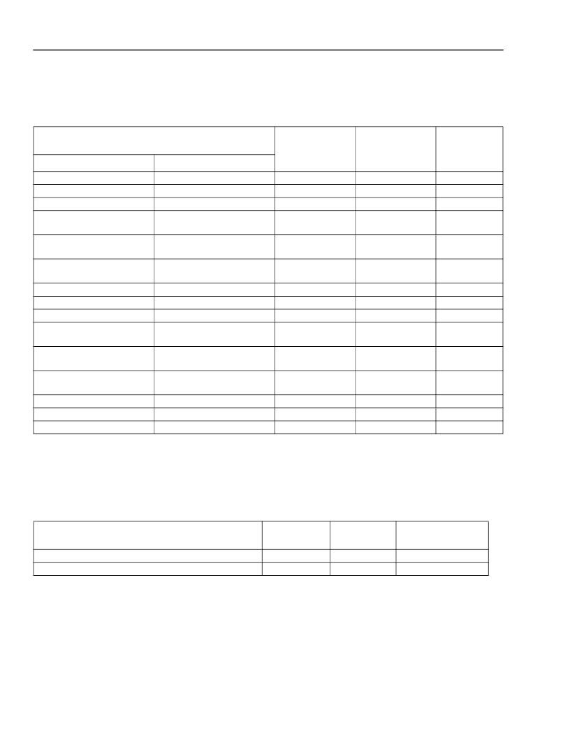
Table 35. OR3TP12 FPGA Side Interface Combinatorial Path Delay Signals
OR3TP12 Commercial: V
DD
= 3.0 V to 3.6 V, 0 °C < T
A
< 70 °C.
Note: The combinatorial path parameters are measured from the input to the output (both on the FPGA side), excluding the interbufs, which
traverse the ASIC/FPGA boundary. The ORCA Foundry static analysis tool, trace, accounts for clock skew and interbuf delays on
the clock and data paths.
Table 36. OR3TP12 Interbuf Delays
OR3TP12 Commercial: V
DD
= 3.0 V to 3.6 V, 0 °C < T
A
< 70 °C.
Note: The interbufs are buffers that interface between the FPGA and the ASIC.
Description
(T
I
= 85 °C, V
DD
= min, V
DD
2 = min)
Min
Max
Unit
Source
fifo_sel
fifo_sel
twdataenn
twdataenn
Destination
datatofpga[31:0]
datatofpgax[3:0]
twlastcycn
datatofpga[31:0]
(dual-port mode)
datatofpgax[3:0]
(dual-port mode)
twdata[17:0]
(quad-port mode)
trlastcycn
mrlastcycn
twlastcycn
datatofpga[31:0]
(dual-port mode)
datatofpgax[3:0]
(dual-port mode)
twdata[17:0]
(quad-port mode)
pci_cfg_stat
datatofpga[31:0]
mrdata[17:0]
—
—
—
—
2.364
1.999
6.565
8.968
ns
ns
ns
ns
twdataenn
—
7.929
ns
twdataenn
—
7.687
ns
trdataenn
mrdataenn
taenn
taenn
—
—
—
—
5.457
5.899
6.530
9.278
ns
ns
ns
ns
taenn
—
7.904
ns
taenn
—
7.696
ns
cfgshiftenn
mrdataenn
mrdataenn
—
—
—
6.202
7.516
7.340
ns
ns
ns
Description
(T
I
= 85 °C, V
DD
= min, V
DD
2 = min)
Interbuf from FPGA to ASIC
Interbuf from ASIC to FPGA
Min
Max
Unit
—
—
0.696
0.505
ns
ns
發(fā)布緊急采購,3分鐘左右您將得到回復(fù)。