- 您現(xiàn)在的位置:買賣IC網(wǎng) > PDF目錄370849 > M37902FCCHP (Mitsubishi Electric Corporation) SINGLE-CHIP 16-BIT CMOS MICROCOMPUTER PDF資料下載
參數(shù)資料
| 型號: | M37902FCCHP |
| 廠商: | Mitsubishi Electric Corporation |
| 英文描述: | SINGLE-CHIP 16-BIT CMOS MICROCOMPUTER |
| 中文描述: | 單片16位CMOS微機 |
| 文件頁數(shù): | 64/143頁 |
| 文件大小: | 1463K |
| 代理商: | M37902FCCHP |
第1頁第2頁第3頁第4頁第5頁第6頁第7頁第8頁第9頁第10頁第11頁第12頁第13頁第14頁第15頁第16頁第17頁第18頁第19頁第20頁第21頁第22頁第23頁第24頁第25頁第26頁第27頁第28頁第29頁第30頁第31頁第32頁第33頁第34頁第35頁第36頁第37頁第38頁第39頁第40頁第41頁第42頁第43頁第44頁第45頁第46頁第47頁第48頁第49頁第50頁第51頁第52頁第53頁第54頁第55頁第56頁第57頁第58頁第59頁第60頁第61頁第62頁第63頁當(dāng)前第64頁第65頁第66頁第67頁第68頁第69頁第70頁第71頁第72頁第73頁第74頁第75頁第76頁第77頁第78頁第79頁第80頁第81頁第82頁第83頁第84頁第85頁第86頁第87頁第88頁第89頁第90頁第91頁第92頁第93頁第94頁第95頁第96頁第97頁第98頁第99頁第100頁第101頁第102頁第103頁第104頁第105頁第106頁第107頁第108頁第109頁第110頁第111頁第112頁第113頁第114頁第115頁第116頁第117頁第118頁第119頁第120頁第121頁第122頁第123頁第124頁第125頁第126頁第127頁第128頁第129頁第130頁第131頁第132頁第133頁第134頁第135頁第136頁第137頁第138頁第139頁第140頁第141頁第142頁第143頁
M37902FCCHP, M37902FGCHP, M37902FJCHP
SINGLE-CHIP 16-BIT CMOS MICROCOMPUTER
MITSUBISHI MICROCOMPUTERS
64
Serial I/O mode select bits
0 0 0 : Serial I/O is invalid. (Port P8 functions as a programmable I/O port.)
0 0 1 : Clock synchronous
1 0 0 : 7-bit UART
1 0 1 : 8-bit UART
1 1 0 : 9-bit UART
Internal/External clock select bit
0 : Internal clock
1 : External clock
Stop bit length select bit (Valid in UART mode.)
0 : 1 stop bit
1 : 2 stop bits
Odd/Even parity select bit (Valid in UART mode with the parity enable bit = “1”.)
(Note)
0 : Odd parity
1 : Even parity
Parity enable bit (Valid in UART mode)
(Note)
0 : No parity
1 : With parity
Sleep select bit (Valid in UART mode)
(Note)
0 : No sleep
1 : Sleep
Note:
In the clock synchronous serial I/O mode, bits 4 to 6 are invalid. (Each of them may be “0” or “1”.) Furthermore, fix bit 7 to “0”.
7 6 5 4 3 2 1 0
UART 0 Transmit/Receive mode register
UART 1 Transmit/Receive mode register
Addresses
30
16
38
16
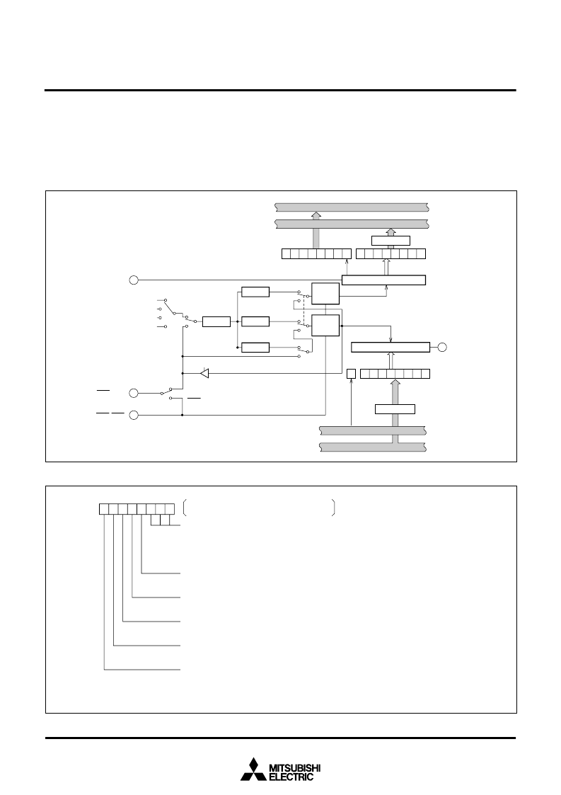
SERIAL I/O PORTS
Two independent serial I/O ports are provided. Figure 64 shows a
block diagram of the serial I/O ports.
Bits 0 to 2 of the UARTi(i = 0,1) transmit/receive mode register
shown in Figure 65 are used to determine whether to use port P8 as
a programmable I/O port, clock synchronous serial I/O port, or asyn-
chronous (UART) serial I/O port which uses start and stop bits.
Figures 66 and 67 show the block diagrams of the receiver/transmit-
ter .
Figure 68 shows the bit configuration of the UARTi transmit/receive
control register.
Each communication method is described below.
Fig. 65 Bit configuration of UARTi transmit/receive mode register
Fig. 64 Block diagram of serial I/O port
UARTi receive register
T
X
D
i
R
X
D
i
Receive
control
circuit
Transmit
control
circuit
UARTi transmit register
1/16 divider
Clock synchronous
1/2 divider
1/(n + 1) divider
1/16 divider
Clock synchronous
Clock synchronous
Transfer clock
Transfer clock
UARTi
transmit buffer register
UART0 (Addresses 33
16
, 32
16
)
UART1 (Addresses 3B
16
, 3A
16
)
UART
Clock synchronous (when internal clock selected)
BRG count source select bits
f
2
f
16
f
64
f
512
(Internal clock)
UART
D
7
D
6
D
5
D
4
D
3
D
2
D
1
UARTi
receive buffer register
D
0
D
7
D
8
D
6
D
5
D
4
D
3
D
2
D
1
D
0
0 D
8
0
0
0
0
0
0
BRGi
UART0 (Addresses 37
16,
36
16
)
UART1 (Addresses 3F
16
, 3E
16
)
CTS
i
/RTS
i
Clock synchronous
(External clock)
n = a value set into the UARTi baud rate register (BRGi)
CLK
i
CTS
i
CTS
i
/CLK
i
Data bus (even)
Data bus (odd)
Bit converter
Data bus (odd)
Data bus (even)
Bit converter
相關(guān)PDF資料 |
PDF描述 |
|---|---|
| M37902FGCHP | DIODE SCHOTTKY DUAL COMMON-ANODE 25V 150mW 0.32V-vf 200mA-IFM 1mA-IF 2uA-IR SOT-523 3K/REEL |
| M37902FJCHP | SINGLE-CHIP 16-BIT CMOS MICROCOMPUTER |
| M37905F8CFP | 16-BIT CMOS MICROCOMPUTER |
| M37905F8CSP | 16-BIT CMOS MICROCOMPUTER |
| M37905M4C | DIODE SCHOTTKY DUAL COMMON-ANODE 25V 200mW 0.32V-vf 200mA-IFM 1mA-IF 2uA-IR SOT-323 3K/REEL |
相關(guān)代理商/技術(shù)參數(shù) |
參數(shù)描述 |
|---|---|
| M37902FGCGP | 制造商:MITSUBISHI 制造商全稱:Mitsubishi Electric Semiconductor 功能描述:SINGLE-CHIP 16-BIT CMOS MICROCOMPUTER |
| M37902FGCHP | 制造商:MITSUBISHI 制造商全稱:Mitsubishi Electric Semiconductor 功能描述:SINGLE-CHIP 16-BIT CMOS MICROCOMPUTER |
| M37902FJCHP | 制造商:MITSUBISHI 制造商全稱:Mitsubishi Electric Semiconductor 功能描述:SINGLE-CHIP 16-BIT CMOS MICROCOMPUTER |
| M37903S4CHP | 制造商:RENESAS 制造商全稱:Renesas Technology Corp 功能描述:16-BIT CMOS MICROCOMPUTER |
| M37905F8CFP | 制造商:MITSUBISHI 制造商全稱:Mitsubishi Electric Semiconductor 功能描述:16-BIT CMOS MICROCOMPUTER |
發(fā)布緊急采購,3分鐘左右您將得到回復(fù)。