- 您現(xiàn)在的位置:買賣IC網(wǎng) > PDF目錄370849 > M37902F8CHP (Mitsubishi Electric Corporation) DIODE SCHOTTKY DUAL COMMON-ANODE 25V 200mW 0.32V-vf 200mA-IFM 1mA-IF 2uA-IR SOT-23 3K/REEL PDF資料下載
參數(shù)資料
| 型號: | M37902F8CHP |
| 廠商: | Mitsubishi Electric Corporation |
| 英文描述: | DIODE SCHOTTKY DUAL COMMON-ANODE 25V 200mW 0.32V-vf 200mA-IFM 1mA-IF 2uA-IR SOT-23 3K/REEL |
| 中文描述: | 單片16位CMOS微機(jī) |
| 文件頁數(shù): | 53/143頁 |
| 文件大小: | 1463K |
| 代理商: | M37902F8CHP |
第1頁第2頁第3頁第4頁第5頁第6頁第7頁第8頁第9頁第10頁第11頁第12頁第13頁第14頁第15頁第16頁第17頁第18頁第19頁第20頁第21頁第22頁第23頁第24頁第25頁第26頁第27頁第28頁第29頁第30頁第31頁第32頁第33頁第34頁第35頁第36頁第37頁第38頁第39頁第40頁第41頁第42頁第43頁第44頁第45頁第46頁第47頁第48頁第49頁第50頁第51頁第52頁當(dāng)前第53頁第54頁第55頁第56頁第57頁第58頁第59頁第60頁第61頁第62頁第63頁第64頁第65頁第66頁第67頁第68頁第69頁第70頁第71頁第72頁第73頁第74頁第75頁第76頁第77頁第78頁第79頁第80頁第81頁第82頁第83頁第84頁第85頁第86頁第87頁第88頁第89頁第90頁第91頁第92頁第93頁第94頁第95頁第96頁第97頁第98頁第99頁第100頁第101頁第102頁第103頁第104頁第105頁第106頁第107頁第108頁第109頁第110頁第111頁第112頁第113頁第114頁第115頁第116頁第117頁第118頁第119頁第120頁第121頁第122頁第123頁第124頁第125頁第126頁第127頁第128頁第129頁第130頁第131頁第132頁第133頁第134頁第135頁第136頁第137頁第138頁第139頁第140頁第141頁第142頁第143頁
53
M37902FCCHP, M37902FGCHP, M37902FJCHP
MITSUBISHI MICROCOMPUTERS
SINGLE-CHIP 16-BIT CMOS MICROCOMPUTER
When bit 2 of the timer Ai mode register is
“
1
”
, the output is gener-
ated from TAi
OUT
pin. The output is toggled each time the contents
of the counter reaches to 0000
16
. When the contents of the count
start bit is
“
0
”
,
“
L
”
is output from TAi
OUT
pin.
When bit 2 is
“
0
”
, TAi
OUT
can be used as a normal port pin. When bit
4 is
“
0
”
, TAi
IN
can be used as a normal port pin.
When bit 4 is
“
1
”
, counting is performed only while the input signal
from the TAi
IN
pin is
“
H
”
or
“
L
”
as shown in Figure 45. Therefore, this
can be used to measure the pulse width of the TAi
IN
input signal.
Whether to count while the input signal is
“
H
”
or while it is
“
L
”
is de-
termined by bit 3. If bit 3 is
“
1
”
, counting is performed while the TAi
IN
pin input signal is
“
H
”
and if bit 3 is
“
0
”
, counting is performed while it
is
“
L
”
.
Note that, the duration of
“
H
”
or
“
L
”
on the TAi
IN
pin must be 2 or
more cycles of the timer count source.
When data is written to timer Ai register with timer Ai halted, the
same data is also written to the reload register and the counter.
When data is written to timer Ai which is busy, the data is written to
the reload register, but not to the counter. The new data is reloaded
from the reload register to the counter at the next reload time and
counting continues. The contents of the counter can be read at any
time.
When the value set in the timer Ai register is n, the timer frequency
division ratio is 1/(n+1).
0 0 : Always
“
00
”
in timer mode
0 : No pulse output (TAi
OUT
is normal port pin.)
1 : Pulse output (TAi
OUT
is pulse output pin.)
(Note)
0
×
: No gate function (TAi
IN
is normal port pin.)
1 0 : Count only while TAi
IN
input is
“
L
”
.
1 1 : Count only while TAi
IN
input is
“
H
”
.
0 : Always
“
0
”
in timer mode.
Clock source select bits
See Table 12.
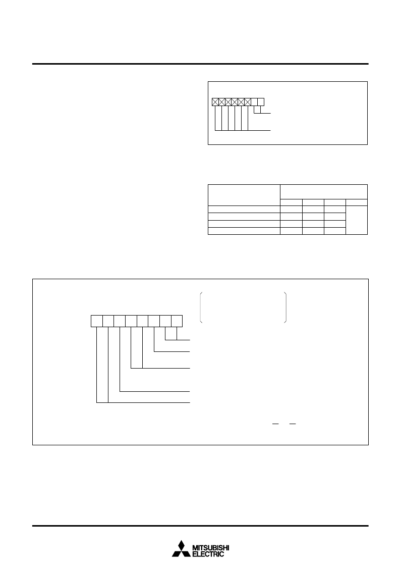
Timer A0 mode register
Timer A1 mode register
Timer A2 mode register
Timer A3 mode register
Timer A4 mode register
7
0
0
6
5
4
3
2
1
0
Addresses
56
16
57
16
58
16
59
16
5A
16
0
Note:
When using pins TA2
OUT
and TA3
OUT
as pulse output pins, do not select pins KI
0
and KI
2
.
Because they are key input interrupt pins and are multiplexed with pins TA2
OUT
and TA3
OUT
.
Fig. 43 Bit configuration of timer Ai mode register during timer mode
Fig. 42 Bit configuration of timer A clock division select register
Table 12. Relationship between timer A clock division select bits,
clock source select bits, and count source
Clock source select bits
(bits 7 and 6 at addresses
56
16
to 5A
16
)
0 0
0 1
f
16
f
64
1 1
f
512
Note:
Timers A0 to A4 use the same clock, which is selected by the
timer A clock division select bits.
Timer A clock division select bit
(See Table 12.)
7 6 5 4 3 2 1 0
Timer A clock division select register
Address
45
16
“
0
”
at read.
1 0
Timer A clock division select bits
(bits 1 and 0 at address 45
16
)
00
f
1
f
16
f
64
f
4096
f
2
01
f
1
f
64
f
512
f
4096
10
11
Do not
select.
相關(guān)PDF資料 |
PDF描述 |
|---|---|
| M37902FGCGP | SINGLE-CHIP 16-BIT CMOS MICROCOMPUTER |
| M37902FCCHP | SINGLE-CHIP 16-BIT CMOS MICROCOMPUTER |
| M37902FGCHP | DIODE SCHOTTKY DUAL COMMON-ANODE 25V 150mW 0.32V-vf 200mA-IFM 1mA-IF 2uA-IR SOT-523 3K/REEL |
| M37902FJCHP | SINGLE-CHIP 16-BIT CMOS MICROCOMPUTER |
| M37905F8CFP | 16-BIT CMOS MICROCOMPUTER |
相關(guān)代理商/技術(shù)參數(shù) |
參數(shù)描述 |
|---|---|
| M37902FCCHP | 制造商:MITSUBISHI 制造商全稱:Mitsubishi Electric Semiconductor 功能描述:SINGLE-CHIP 16-BIT CMOS MICROCOMPUTER |
| M37902FGCGP | 制造商:MITSUBISHI 制造商全稱:Mitsubishi Electric Semiconductor 功能描述:SINGLE-CHIP 16-BIT CMOS MICROCOMPUTER |
| M37902FGCHP | 制造商:MITSUBISHI 制造商全稱:Mitsubishi Electric Semiconductor 功能描述:SINGLE-CHIP 16-BIT CMOS MICROCOMPUTER |
| M37902FJCHP | 制造商:MITSUBISHI 制造商全稱:Mitsubishi Electric Semiconductor 功能描述:SINGLE-CHIP 16-BIT CMOS MICROCOMPUTER |
| M37903S4CHP | 制造商:RENESAS 制造商全稱:Renesas Technology Corp 功能描述:16-BIT CMOS MICROCOMPUTER |
發(fā)布緊急采購,3分鐘左右您將得到回復(fù)。